Results in Physics ( IF 5.3 ) Pub Date : 2021-04-30 , DOI: 10.1016/j.rinp.2021.104250 Weiwei Ju , Yi Zhang , Tongwei Li , Donghui Wang , Enqin Zhao , Guangxiong Hu , Yanmin Xu , Haisheng Li
|
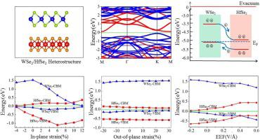
The construction of van der Waals (vdW) heterostructures is an efficient strategy for attaining more desired specifications. According to first-principles calculations, the WSe2/HfSe2 vdW heterostructure has an indirect band gap from K point to M point with the value of 0.21 eV. A conventional type-II band alignment is constructed for the WSe2/HfSe2 heterostructure, where the electrons and holes are placed in HfSe2 and WSe2 layers, respectively, facilitating the efficient separation of photo-generated electron and hole pairs. Although both WSe2 and HfSe2 monolayers were highly insulating, Kashiwabara group found that WSe2/HfSe2 heterostructure were highly conducting [Adv. Funct. Mater. 2019, 29, 1900354]. Our calculated results suggest that the strain and external electric field can lead to the transition from semiconductor to metal, resulting in high conductivity. The band alignment transition from type-II to type-I can also be obtained by means of in-plane strains and external electric field. The interlayer coupling only affects the values of band gap. Moreover, the investigation on the optical properties shows that the optical absorption intensity of WSe2/HfSe2 heterostructure can attain the order of 105. These findings indicate that the WSe2/HfSe2 vdW heterostructure is promising for efficient optoelectronic nanodevices.
中文翻译:
具有可调电子和光学性质的II型WSe 2 / HfSe 2范德华异质结构
范德华(vdW)异质结构的构造是获得更理想规格的有效策略。根据第一性原理计算,WSe 2 / HfSe 2 vdW异质结构具有从K点到M点的间接带隙,其值为0.21 eV。针对WSe 2 / HfSe 2异质结构构建了常规的II型能带排列,其中电子和空穴分别置于HfSe 2和WSe 2层中,从而促进了光生电子和空穴对的有效分离。虽然WSe 2和HfSe 2单层都是高度绝缘的,但柏原研究小组发现WSe 2和HfSe 2单层都具有很高的绝缘性。2 / HfSe 2异质结构具有高传导性[ Adv。功能 母校 2019,29,1900354]。我们的计算结果表明,应变和外部电场可导致从半导体到金属的过渡,从而导致高电导率。从II型到I型的能带取向转变也可以通过面内应变和外部电场来获得。层间耦合仅影响带隙的值。此外,对光学性质的研究表明,WSe 2 / HfSe 2异质结构的光吸收强度可以达到10 5数量级。这些发现表明WSe 2 / HfSe 2 vdW异质结构有望用于高效的光电纳米器件。


 京公网安备 11010802027423号