当前位置:
X-MOL 学术
›
Phys. Rev. Research
›
论文详情
Our official English website, www.x-mol.net, welcomes your feedback! (Note: you will need to create a separate account there.)
Topoelectric circuits: Theory and construction
Physical Review Research Pub Date : 2021-04-19 , DOI: 10.1103/physrevresearch.3.023056 Junkai Dong , Vladimir Juričić , Bitan Roy
Physical Review Research Pub Date : 2021-04-19 , DOI: 10.1103/physrevresearch.3.023056 Junkai Dong , Vladimir Juričić , Bitan Roy
|
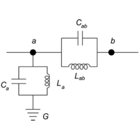
We highlight a general theory to engineer arbitrary Hermitian tight-binding lattice models in electrical LC circuits, where the lattice sites are replaced by the electrical nodes, connected to its neighbors and to the ground by capacitors and inductors. In particular, by supplementing each node with subnodes, where the phases of the current and voltage are the distinct roots of unity, one can in principle realize arbitrary hopping amplitude between the sites or nodes via the shift capacitor coupling between them. This general principle is then implemented to construct a plethora of topological models in electrical circuits, topolectric circuits, where the robust zero-energy topological boundary modes manifest through a large boundary impedance, when the circuit is tuned to the resonance frequency. The simplicity of our circuit constructions is based on the fact that the existence of the boundary modes relies only on the Clifford algebra of the corresponding Hermitian matrices entering the Hamiltonian and not on their particular representation. This in turn enables us to implement a wide class of topological models through rather simple topolectric circuits with nodes consisting of only two subnodes. We anchor these outcomes from the numerical computation of the on-resonance impedance in circuit realizations of first-order (), such as Chern and quantum spin Hall insulators, and second- () and third- () order topological insulators in different dimensions, featuring sharp localization on boundaries of codimensionality . Finally, we subscribe to the stacked topolectric circuit construction to engineer three-dimensional Weyl, nodal-loop, quadrupolar Dirac, and Weyl semimetals, respectively, displaying surface- and hinge-localized impedance.
中文翻译:

拓扑电路:理论与构造
我们着重介绍了在电气LC电路中设计任意Hermitian紧束缚晶格模型的一般理论,其中晶格位置被电气节点取代,电气节点连接到其邻居,并通过电容器和电感器接地。特别是,通过向每个节点补充 子节点,其中电流和电压的相位是 在单位制的不同根源上,原则上可以通过站点或节点之间的移位电容器耦合来实现站点或节点之间的任意跳变幅度。然后实施该一般原理,以构造电路,极电回路中的大量拓扑模型,当电路调谐至谐振频率时,稳健的零能量拓扑边界模式通过较大的边界阻抗体现出来。我们的电路构造的简单性是基于这样一个事实,即边界模态的存在仅取决于进入哈密顿量的相应厄米矩阵的Clifford代数,而不是它们的特定表示。反过来,这使我们能够通过相当简单的极点电路来实现各种拓扑模型,这些极点电路的节点仅由两个子节点组成。我们根据一阶(),例如Chern和量子自旋霍尔绝缘子,以及第二个-()和第三个()订购具有不同尺寸的拓扑绝缘子,在共维数边界上具有鲜明的局部性 。最后,我们订阅了堆叠式极点电路构造,分别设计了三维Weyl,节点环,四极Dirac和Weyl半金属,以显示表面和铰链局部阻抗。
更新日期:2021-04-19
中文翻译:
拓扑电路:理论与构造
我们着重介绍了在电气LC电路中设计任意Hermitian紧束缚晶格模型的一般理论,其中晶格位置被电气节点取代,电气节点连接到其邻居,并通过电容器和电感器接地。特别是,通过向每个节点补充 子节点,其中电流和电压的相位是 在单位制的不同根源上,原则上可以通过站点或节点之间的移位电容器耦合来实现站点或节点之间的任意跳变幅度。然后实施该一般原理,以构造电路,极电回路中的大量拓扑模型,当电路调谐至谐振频率时,稳健的零能量拓扑边界模式通过较大的边界阻抗体现出来。我们的电路构造的简单性是基于这样一个事实,即边界模态的存在仅取决于进入哈密顿量的相应厄米矩阵的Clifford代数,而不是它们的特定表示。反过来,这使我们能够通过相当简单的极点电路来实现各种拓扑模型,这些极点电路的节点仅由两个子节点组成。我们根据一阶(),例如Chern和量子自旋霍尔绝缘子,以及第二个-()和第三个()订购具有不同尺寸的拓扑绝缘子,在共维数边界上具有鲜明的局部性 。最后,我们订阅了堆叠式极点电路构造,分别设计了三维Weyl,节点环,四极Dirac和Weyl半金属,以显示表面和铰链局部阻抗。


 京公网安备 11010802027423号