Light: Science & Applications ( IF 19.4 ) Pub Date : 2021-04-15 , DOI: 10.1038/s41377-021-00524-7 Ting-Xiao Qin , En-Ming You , Mao-Xin Zhang , Peng Zheng , Xiao-Feng Huang , Song-Yuan Ding , Bing-Wei Mao , Zhong-Qun Tian
|
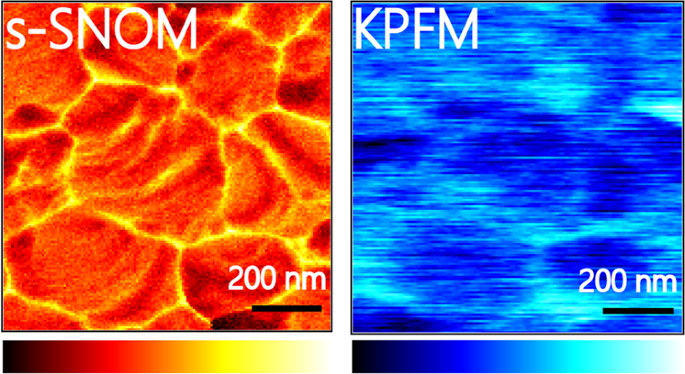
Organic–inorganic halide perovskites are emerging materials for photovoltaic applications with certified power conversion efficiencies (PCEs) over 25%. Generally, the microstructures of the perovskite materials are critical to the performances of PCEs. However, the role of the nanometer-sized grain boundaries (GBs) that universally existing in polycrystalline perovskite films could be benign or detrimental to solar cell performance, still remains controversial. Thus, nanometer-resolved quantification of charge carrier distribution to elucidate the role of GBs is highly desirable. Here, we employ correlative infrared-spectroscopic nanoimaging by the scattering-type scanning near-field optical microscopy with 20 nm spatial resolution and Kelvin probe force microscopy to quantify the density of electrons accumulated at the GBs in perovskite polycrystalline thin films. It is found that the electron accumulations are enhanced at the GBs and the electron density is increased from 6 × 1019 cm−3 in the dark to 8 × 1019 cm−3 under 10 min illumination with 532 nm light. Our results reveal that the electron accumulations are enhanced at the GBs especially under light illumination, featuring downward band bending toward the GBs, which would assist in electron-hole separation and thus be benign to the solar cell performance.
Correlative infrared-spectroscopic nanoimaging by the scattering-type scanning near-field optical microscopy and Kelvin probe force microscopy quantitatively reveal the accumulated electrons at GBs in perovskite polycrystalline thin films.
中文翻译:
通过相关红外光谱纳米成像和开尔文探针力显微镜定量钙钛矿多晶膜中晶界电子的积累
有机-无机卤化物钙钛矿是新兴的光伏应用材料,其认证的功率转换效率(PCE)超过25%。通常,钙钛矿材料的微观结构对PCE的性能至关重要。然而,普遍存在于多晶钙钛矿薄膜中的纳米级晶界(GBs)的作用可能对太阳能电池的性能是良性的或有害的,仍然是有争议的。因此,非常需要对纳米级解析的电荷载流子分布进行量化,以阐明GBs的作用。这里,我们通过散射型扫描近场光学显微镜(具有20 nm的空间分辨率)和Kelvin探针力显微镜,采用相关的红外光谱纳米成像技术来量化钙钛矿多晶薄膜中在GBs处积累的电子密度。发现在GBs处电子积累增加,电子密度从6×10增加19 厘米-3在黑暗中8×10 19 厘米-3下10分钟与照明532纳米的光。我们的结果表明,尤其是在光照射下,电子在GBs处的蓄积得到了增强,其特征是朝GBs的向下带弯曲,这将有助于电子-空穴的分离,因此对太阳能电池的性能是有益的。
通过散射型扫描近场光学显微镜和开尔文探针力显微镜的相关红外光谱纳米成像定量地揭示了钙钛矿多晶薄膜中GBs处的累积电子。


 京公网安备 11010802027423号