Extreme Mechanics Letters ( IF 4.7 ) Pub Date : 2021-03-26 , DOI: 10.1016/j.eml.2021.101287 Byoung-Joo Lee , Dahl-Young Khang
|
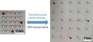
Non-deterministic transfer printing of LED chips with controllable pitch has been demonstrated. An elastomeric stamp with pillars array, after picking up the corresponding array of chips, has been stretched and then the chip array was transfer-printed onto a receiver substrate, so that the pitch between chips can be controllably varied. The controllable pitch in the proposed non-deterministic transfer process can reduce the number of transfer down to 1/3 compared to other deterministic transfer techniques, which can greatly reduce the production time for full color LED displays. For the successful implementation of the non-deterministic transfer printing, stamp design has been optimized and verified by both experiments and finite element analysis. Specifically, pillar-patterned stamp has been found to reduce strain on pillar top down to 1/10 by the localization of applied strain onto inter-pillar regions. Further, re-entrant geometry of pillars can reduce the strain on pillar top additionally, leading to the protection of chips arrangement on pillared stamp upon very large stretching of 100200% or more. Deformation mechanics of stamp with various pillar geometries have been analyzed for uni- or bi-axial strain, which shows reasonable agreement with experimental findings. Based on the developed non-deterministic transfer process, stretchable LED array has been successfully demonstrated, without deteriorating the performance upon stretching. The non-deterministic transfer printing technique developed in this work may be a valuable help for enhancing the productivity of LED-based displays.
中文翻译:
使用可伸展的弹性印章以可控制的间距进行不确定的LED芯片转印
已经证明了间距可控的LED芯片的不确定性转移印刷。在拾取相应的芯片阵列之后,具有支柱阵列的弹性压模被拉伸,然后将芯片阵列转移打印到接收器基板上,从而可以控制芯片之间的间距。与其他确定性转移技术相比,在所提出的非确定性转移过程中可控的间距可以将转移次数减少到1/3,从而可以大大减少全彩LED显示器的生产时间。为了成功实施非确定性转移印刷,已通过实验和有限元分析对印章设计进行了优化和验证。具体来说,发现柱状图章可将柱顶上的应变降低到通过将施加的应变局部化到柱间区域上来获得1/10。此外,支柱的凹入几何形状还可以减少支柱顶部的应变,从而在100的非常大的拉伸时导致保护在支柱邮票上的切屑排列200%以上。已经分析了具有各种支柱几何形状的邮票的变形力学的单轴或双轴应变,这与实验结果显示出合理的一致性。基于已开发的非确定性转移工艺,可拉伸的LED阵列已被成功演示,而不会降低拉伸时的性能。这项工作中开发的非确定性转移打印技术可能对提高基于LED的显示器的生产率很有帮助。


 京公网安备 11010802027423号