当前位置:
X-MOL 学术
›
Laser Photonics Rev.
›
论文详情
Our official English website, www.x-mol.net, welcomes your feedback! (Note: you will need to create a separate account there.)
Micro‐Light Emitting Diode: From Chips to Applications
Laser & Photonics Reviews ( IF 11.0 ) Pub Date : 2021-03-24 , DOI: 10.1002/lpor.202000133 Peter J. Parbrook 1, 2 , Brian Corbett 1 , Jung Han 3 , Tae‐Yeon Seong 4 , Hiroshi Amano 5
Laser & Photonics Reviews ( IF 11.0 ) Pub Date : 2021-03-24 , DOI: 10.1002/lpor.202000133 Peter J. Parbrook 1, 2 , Brian Corbett 1 , Jung Han 3 , Tae‐Yeon Seong 4 , Hiroshi Amano 5
Affiliation
|
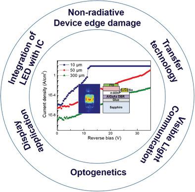
Typical light‐emitting diodes (LEDs) have a form factor >(300 × 300) µm2. Such LEDs are commercially mature in illumination and ultralarge displays. However, recent LED research includes shrinking individual LED sizes from side lengths >300 µm to values <100 µm, leading to devices called micro‐LEDs. Their advent creates a number of exciting new application spaces. Here, a review of the principles and applications of micro‐LED technology is presented. In particular, the implications of reduced LED size in necessitating mitigation strategies for nonradiative device edge damage as well as the potential for higher drive current densities are discussed. The opportunities to integrate micro‐LEDs with electronics, and into large‐scale arrays, allow pixel addressable scalable integrated displays, while the small micro‐LED size is ideal for high‐speed modulation for visible light communication, and for integration into biological systems as part of optogenetic therapies.
中文翻译:

微发光二极管:从芯片到应用
典型的发光二极管(LED)的尺寸系数>(300×300)µm 2。这样的LED在照明和超大型显示器中在商业上已经成熟。但是,最近的LED研究包括将单个LED的尺寸从侧面长度> 300 µm减小到值<100 µm,从而导致了被称为微型LED的设备。他们的出现创造了许多令人兴奋的新应用空间。在这里,对Micro-LED技术的原理和应用进行了概述。尤其是,讨论了减小LED尺寸对于必须采取缓解策略以防止非辐射性器件边缘损坏以及更高驱动电流密度的可能性所带来的影响。将Micro-LED与电子设备集成并集成到大规模阵列中的机会使像素可寻址的可扩展集成显示器成为可能,而较小的Micro-LED尺寸则是用于可见光通信的高速调制的理想选择,
更新日期:2021-05-07
中文翻译:
微发光二极管:从芯片到应用
典型的发光二极管(LED)的尺寸系数>(300×300)µm 2。这样的LED在照明和超大型显示器中在商业上已经成熟。但是,最近的LED研究包括将单个LED的尺寸从侧面长度> 300 µm减小到值<100 µm,从而导致了被称为微型LED的设备。他们的出现创造了许多令人兴奋的新应用空间。在这里,对Micro-LED技术的原理和应用进行了概述。尤其是,讨论了减小LED尺寸对于必须采取缓解策略以防止非辐射性器件边缘损坏以及更高驱动电流密度的可能性所带来的影响。将Micro-LED与电子设备集成并集成到大规模阵列中的机会使像素可寻址的可扩展集成显示器成为可能,而较小的Micro-LED尺寸则是用于可见光通信的高速调制的理想选择,


 京公网安备 11010802027423号