Micro and Nanostructures ( IF 3.1 ) Pub Date : 2021-03-06 , DOI: 10.1016/j.spmi.2021.106858 Radha N Somaiya , Yogesh Sonvane , Sanjeev K. Gupta
|
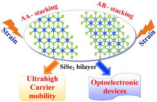
Here, we have studied the electronic transport and optical properties of recently predicted SiSe2 homo-bilayer considering two stacking sequences. To confirm its dynamical stability, phonon spectrum is studied and shows that both AA- and AB-stackings are thermodynamically stable. Both the stackings show indirect characteristics with a band gap of 1.12 eV and 0.99 eV calculated with HSE06 hybrid functional. Higher electron carrier mobilities of the order of 103 cm2V−1sec−1 are obtained along x- and y-direction for both the stackings indicating n-type electronic characteristics. Higher values of electronic mobilities mainly arise out of lower deformation potentials. On application of biaxial compressive strains of about −5%, the bilayer encounters a transition and becomes metal. Furthermore, the absorption spectrum indicates a wide area covered. Small absorption can be observed in the near IR, visible and UV-region indicating its usefulness in the nano-optoelectronic device applications. Our results show that strain plays an important role due to lattice mismatching and can be used in future nano-optoelectronic devices.
中文翻译:
Van der Waals将SiSe 2同质双分子层用于光电应用
在这里,我们研究了考虑到两个堆叠序列的最近预测的SiSe 2同质双分子层的电子传输和光学性质。为了确认其动态稳定性,对声子谱进行了研究,结果表明AA和AB堆叠都是热力学稳定的。两种堆叠均显示间接特性,其带隙为HSE06混合功能计算的1.12 eV和0.99 eV。较高的电子载流子迁移率约为10 3 cm 2 V -1 sec -1对于表示n型电子特性的两个堆叠,沿着x方向和y方向获得Δθ。电子迁移率的较高值主要来自较低的变形电势。在施加约-5%的双轴压缩应变时,双层遇到过渡并变成金属。此外,吸收光谱表明覆盖的区域很大。在近红外,可见光和紫外区域可以观察到小的吸收,表明其在纳米光电器件应用中的有用性。我们的结果表明,由于晶格失配,应变起着重要的作用,并且可以在未来的纳米光电器件中使用。


 京公网安备 11010802027423号