当前位置:
X-MOL 学术
›
Phys. Status Solidi A
›
论文详情
Our official English website, www.x-mol.net, welcomes your feedback! (Note: you will need to create a separate account there.)
Effect of Source–Drain Electric Field on Charge Transport Mechanism in Polymer-Based Thin-Film Transistors
Physica Status Solidi (A) - Applications and Materials Science ( IF 2 ) Pub Date : 2021-02-25 , DOI: 10.1002/pssa.202000753 Swarup Biswas 1 , Kyeong-Ho Seo 2 , Yongju Lee 1, 3 , Yun-Hi Kim 4 , Jin-Hyuk Bae 2, 5 , Hyeok Kim 1
Physica Status Solidi (A) - Applications and Materials Science ( IF 2 ) Pub Date : 2021-02-25 , DOI: 10.1002/pssa.202000753 Swarup Biswas 1 , Kyeong-Ho Seo 2 , Yongju Lee 1, 3 , Yun-Hi Kim 4 , Jin-Hyuk Bae 2, 5 , Hyeok Kim 1
Affiliation
|
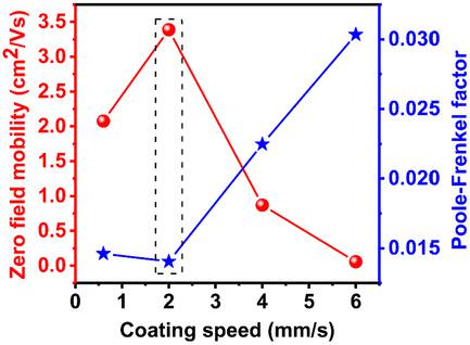
Donor–acceptor copolymer-based field-effect transistors (FETs) have attracted considerable attention from technological and academic perspectives due to their low band gap, high mobility, low cost, and easy solution processability, flexibility, and stretch ability. Among different solution-processing techniques, meniscus-guided coating has the potential for large-area film formation. Moreover, 29-diketopyrrolopyrroleselenophene vinylene selenophene (29-DPP-SVS) donor-acceptor copolymer-based FETs have already exhibited excellent performance due to their short π–π stacking distance and strong π–π interaction. Charge carrier mobility of these types of semiconducting materials is significantly dependent on the applied electric field. Therefore, detailed analysis of the electric-field dependency of charge carrier mobility is necessary to understand the transport mechanisms within these materials. Thus, herein, 29-DPP-SVS-based FETs are fabricated by varying the blade-coating speed of their semiconductor layer. Then, the effect of the blade-coating speed on the electrical properties of the FETs is studied through the analysis of electric-field-dependent mobility. The results suggest that the charge carrier mobility of different FETs is dependent on the applied electric field and that the type of dependency is Poole–Frenkel. At an optimized blade-coating speed (2 mm s−1), the device exhibits maximum zero-field mobility (3.39 cm2 V−1 s−1) due to the low trap density within the conducting channel.
中文翻译:

源漏电场对聚合物基薄膜晶体管电荷传输机制的影响
基于供体-受体共聚物的场效应晶体管(FET)由于其低带隙、高迁移率、低成本以及易于溶液加工、柔韧性和拉伸能力而从技术和学术角度引起了广泛关注。在不同的溶液处理技术中,弯液面引导涂层具有大面积成膜的潜力。此外,基于 29-二酮吡咯并吡咯硒吩烯 (29-DPP-SVS) 供体-受体共聚物的 FET 由于其短的 π-π 堆积距离和强的 π-π 相互作用已经表现出优异的性能。这些类型的半导体材料的电荷载流子迁移率显着取决于施加的电场。所以,详细分析电荷载流子迁移率的电场依赖性对于理解这些材料内的传输机制是必要的。因此,在此,通过改变其半导体层的刮涂速度来制造基于 29-DPP-SVS 的 FET。然后,通过对电场相关迁移率的分析,研究了刮刀涂布速度对 FET 电性能的影响。结果表明,不同 FET 的电荷载流子迁移率取决于施加的电场,并且依赖性类型是 Poole-Frenkel。以优化的刮刀涂布速度 (2 mm s 通过对电场相关迁移率的分析,研究了刮刀涂布速度对 FET 电性能的影响。结果表明,不同 FET 的电荷载流子迁移率取决于施加的电场,并且依赖性类型是 Poole-Frenkel。以优化的刮刀涂布速度 (2 mm s 通过对电场相关迁移率的分析,研究了刮刀涂布速度对 FET 电性能的影响。结果表明,不同 FET 的电荷载流子迁移率取决于施加的电场,并且依赖性类型是 Poole-Frenkel。以优化的刮刀涂布速度 (2 mm s-1 ),由于导电通道内的低陷阱密度,该器件表现出最大的零场迁移率(3.39 cm 2 V -1 s -1)。
更新日期:2021-02-25
中文翻译:
源漏电场对聚合物基薄膜晶体管电荷传输机制的影响
基于供体-受体共聚物的场效应晶体管(FET)由于其低带隙、高迁移率、低成本以及易于溶液加工、柔韧性和拉伸能力而从技术和学术角度引起了广泛关注。在不同的溶液处理技术中,弯液面引导涂层具有大面积成膜的潜力。此外,基于 29-二酮吡咯并吡咯硒吩烯 (29-DPP-SVS) 供体-受体共聚物的 FET 由于其短的 π-π 堆积距离和强的 π-π 相互作用已经表现出优异的性能。这些类型的半导体材料的电荷载流子迁移率显着取决于施加的电场。所以,详细分析电荷载流子迁移率的电场依赖性对于理解这些材料内的传输机制是必要的。因此,在此,通过改变其半导体层的刮涂速度来制造基于 29-DPP-SVS 的 FET。然后,通过对电场相关迁移率的分析,研究了刮刀涂布速度对 FET 电性能的影响。结果表明,不同 FET 的电荷载流子迁移率取决于施加的电场,并且依赖性类型是 Poole-Frenkel。以优化的刮刀涂布速度 (2 mm s 通过对电场相关迁移率的分析,研究了刮刀涂布速度对 FET 电性能的影响。结果表明,不同 FET 的电荷载流子迁移率取决于施加的电场,并且依赖性类型是 Poole-Frenkel。以优化的刮刀涂布速度 (2 mm s 通过对电场相关迁移率的分析,研究了刮刀涂布速度对 FET 电性能的影响。结果表明,不同 FET 的电荷载流子迁移率取决于施加的电场,并且依赖性类型是 Poole-Frenkel。以优化的刮刀涂布速度 (2 mm s-1 ),由于导电通道内的低陷阱密度,该器件表现出最大的零场迁移率(3.39 cm 2 V -1 s -1)。


 京公网安备 11010802027423号