International Journal of Machine Tools and Manufacture ( IF 14.0 ) Pub Date : 2021-01-22 , DOI: 10.1016/j.ijmachtools.2021.103701 Jiqiang Wang , Yongda Yan , Zihan Li , Yanquan Geng
|
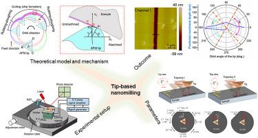
Atomic force microscopy (AFM) tip-based nanofabrication is as a powerful method to machine nanostructures. However, the traditional AFM scratching process suffers from low processing efficiency and a low rate of material removal. Thus, an AFM tip-based nanomilling method was previously proposed to improve the machining efficiency and material removal rate; however, the machining mechanism of the nanomilling process, especially on hard-brittle silicon crystals, is not well understood. In this study, we used an AFM tip-based nanomilling approach to machine nanochannels on single-crystal silicon to investigate the machining mechanism (i.e., the material removal state, undeformed chip thickness, the brittle-to-ductile transition, and subsurface damage). For the first time, we established a theoretical model for tip-based nanomilling with a constant normal load to predict the machined depth. Nanochannels fabricated with a wide range of feed directions, crystal orientations, and tip trajectories were obtained, which provided a reference for machining high-quality nanochannels and an in-depth understanding of the nanomilling of single-crystal silicon. The experimental results demonstrated that we could machine a nanochannel without pile-ups by selecting a specific trajectory with a feed smaller than 4 nm in the 0° direction, a normal load no greater than 120 μN, and a crystal orientation at rotation angles of 135°, 157.5°, or 180°. Moreover, transmission electron microscope analysis of the subsurface of the nanochannel revealed a large number of dislocations, stacking faults, and a layer of amorphous silicon. Our findings are of great significance for obtaining high-quality nanochannels with a predicable machined depth and understanding the nanomilling mechanism of hard-brittle materials.
中文翻译:
旨在了解基于原子力显微镜尖端的纳米铣削加工的加工机理
基于原子力显微镜(AFM)尖端的纳米加工是加工纳米结构的强大方法。然而,传统的AFM刮擦工艺具有低的加工效率和低的材料去除率。因此,先前提出了一种基于AFM尖端的纳米铣削方法,以提高加工效率和材料去除率。但是,纳米铣削加工的机械机理,特别是在脆性硅晶体上的机理尚不十分清楚。在这项研究中,我们使用基于AFM尖端的纳米铣削方法在单晶硅上加工纳米通道,以研究加工机理(即材料去除状态,未变形的切屑厚度,脆性至延性转变以及表面下破坏) 。首次,我们建立了具有恒定法向载荷的基于尖端的纳米铣削的理论模型,以预测加工深度。获得了具有广泛的进给方向,晶体取向和尖端轨迹的纳米通道,这为加工高质量的纳米通道和深入理解单晶硅的纳米铣削提供了参考。实验结果表明,通过选择在0°方向上进给小于4 nm,法向载荷不大于120μN且旋转角度为135时的晶体取向的特定轨迹,我们可以加工出没有堆积的纳米通道°,157.5°或180°。此外,对纳米通道下表面的透射电子显微镜分析显示出大量的位错,堆垛层错和一层非晶硅。


 京公网安备 11010802027423号