当前位置:
X-MOL 学术
›
Small Methods
›
论文详情
Our official English website, www.x-mol.net, welcomes your feedback! (Note: you will need to create a separate account there.)
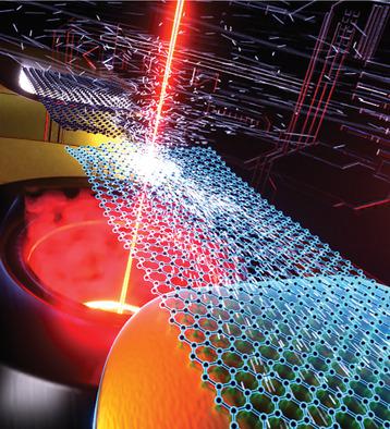
Imaging Secondary Electron Emission from a Single Atomic Layer
Small Methods ( IF 12.4 ) Pub Date : 2021-01-15 , DOI: 10.1002/smtd.202000950 Ondrej Dyck 1 , Jacob L Swett 2 , Andrew R Lupini 1 , Jan A Mol 2, 3 , Stephen Jesse 1
Small Methods ( IF 12.4 ) Pub Date : 2021-01-15 , DOI: 10.1002/smtd.202000950 Ondrej Dyck 1 , Jacob L Swett 2 , Andrew R Lupini 1 , Jan A Mol 2, 3 , Stephen Jesse 1
Affiliation
|
Graphene‐based devices hold promise for a wide range of technological applications. Yet characterizing the structure and the electrical properties of a material that is only one atomic layer thick still poses technical challenges. Recent investigations indicate that secondary‐electron electron‐beam‐induced current (SE‐EBIC) imaging can reveal subtle details regarding electrical conductivity and electron transport with high spatial resolution. Here, it is shown that the SEEBIC imaging mode can be used to detect suspended single layers of graphene and distinguish between different numbers of layers. Pristine and contaminated areas of graphene are also compared to show that pristine graphene exhibits a substantially lower SE yield than contaminated regions. This SEEBIC imaging mode may provide valuable information for the engineering of surface coatings where SE yield is a priority.
中文翻译:

成像来自单个原子层的二次电子发射
基于石墨烯的设备有望用于广泛的技术应用。然而,表征只有一个原子层厚的材料的结构和电学特性仍然存在技术挑战。最近的研究表明,二次电子束诱导电流 (SE-EBIC) 成像可以以高空间分辨率揭示有关电导率和电子传输的细微细节。这里表明,SEEBIC 成像模式可用于检测悬浮的单层石墨烯并区分不同的层数。还比较了石墨烯的原始区域和污染区域,以表明原始石墨烯的 SE 产率显着低于污染区域。
更新日期:2021-01-15
中文翻译:
成像来自单个原子层的二次电子发射
基于石墨烯的设备有望用于广泛的技术应用。然而,表征只有一个原子层厚的材料的结构和电学特性仍然存在技术挑战。最近的研究表明,二次电子束诱导电流 (SE-EBIC) 成像可以以高空间分辨率揭示有关电导率和电子传输的细微细节。这里表明,SEEBIC 成像模式可用于检测悬浮的单层石墨烯并区分不同的层数。还比较了石墨烯的原始区域和污染区域,以表明原始石墨烯的 SE 产率显着低于污染区域。


 京公网安备 11010802027423号