Cell Reports Physical Science ( IF 8.9 ) Pub Date : 2021-01-06 , DOI: 10.1016/j.xcrp.2020.100298 Yue Zheng , Jing Gao , Cheng Han , Wei Chen
|
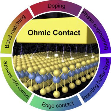
One of the major areas of semiconductor device research is the development of transparent or ohmic contacts between semiconductors and metal electrodes for the efficient injection of charge carriers into the conduction channel. Fast-emerging two-dimensional (2D) materials with atomically flat surfaces, free of dangling bonds, are intuitively promising to form ohmic contacts with metals. However, the contacts of 2D devices usually possess a large Schottky barrier and rarely follow the Schottky-Mott rule, because of interfacial effects such as Fermi-level pinning. Herein, we summarize recent progress and developments in contact engineering of 2D materials for the realization of ohmic contacts in 2D electronic devices. The basic physics of contacts for both Si and 2D materials is briefly introduced. A variety of engineering strategies are subsequently introduced, including band matching, doping, phase engineering, insertion of buffer layers, 2D/metal van der Waals contacts, and edge contacts. Finally, opportunities and challenges for optimizing contacts for future 2D electronics are discussed.
中文翻译:
二维材料的欧姆接触工程
半导体器件研究的主要领域之一是开发半导体和金属电极之间的透明或欧姆接触,以将电荷载流子有效注入导电通道。具有原子平面的无悬空键的快速出现的二维(2D)材料直观上有望与金属形成欧姆接触。然而,由于诸如费米能级钉扎的界面效应,二维设备的触点通常具有较大的肖特基势垒,并且很少遵循肖特基-莫特规则。在此,我们总结了用于实现2D电子设备中的欧姆接触的2D材料接触工程的最新进展和发展。简要介绍了Si和2D材料接触的基本物理原理。随后引入了多种工程策略,包括能带匹配,掺杂,相位工程,缓冲层的插入,2D /金属范德华接触和边缘接触。最后,讨论了优化未来2D电子设备接触的机遇和挑战。


 京公网安备 11010802027423号