International Journal of Machine Tools and Manufacture ( IF 14.0 ) Pub Date : 2021-01-02 , DOI: 10.1016/j.ijmachtools.2020.103688 Weihai Huang , Jiwang Yan
|
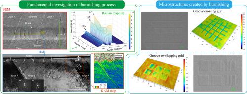
Brittle crystalline materials have important applications in optics and optoelectronics. However, their powders are highly toxic; thus, the chips generated in material removal processes such as cutting, grinding, and polishing are harmful to human health and the environment. In this study, micro/nanoscale burnishing tests were conducted on polycrystalline zinc selenide (p-ZnSe) to explore the feasibility of high-precision surface patterning of a toxic material by local plastic deformation without chip generation. The local deformation behaviours and subsurface damage formation mechanisms were investigated under dry and oil-lubricated conditions. Two types of cracks occurred when the force exceeded a critical value: cracks along the slip planes at the groove bottom and cracks along the cleavage planes at the groove edge. Below the critical force value, however, a crack-free surface was obtained with lower surface roughness than those for diamond-turned surfaces. No phase transformation was detected after burnishing, but lattice distortion appeared in the subsurface layer. A model was developed to predict the activated slip planes by calculating the maximum Schmid factors of the slip systems, and the distribution of subsurface defects was clarified by cross-sectional direct observations. It was also found that the use of a lubricating oil could greatly reduce material pile-ups around the tool. As test pieces, microgrid patterns were fabricated by crossing and overlapping the grooves, and smooth surfaces with surface roughness of 1.85 nm Sa and 4.5 nm Sa, respectively, were achieved. The findings from this study demonstrate the feasibility of chip-free surface patterning on toxic brittle polycrystalline materials by micro/nanoscale burnishing, which is an effective alternative to cutting and grinding for the fabrication of micro structured optical elements and microfluidics.
中文翻译:
通过微/纳米级打磨对有毒脆性多晶材料进行无屑表面图案化
脆性晶体材料在光学和光电子学中具有重要的应用。但是,它们的粉末有剧毒。因此,在切削,打磨和抛光等材料去除过程中产生的切屑对人体健康和环境有害。在这项研究中,对多晶硒化锌(p-ZnSe)探索有毒材料通过局部塑性变形而不产生切屑的高精度表面图案的可行性。研究了在干燥和油润滑条件下的局部变形行为和地下破坏形成机理。当力超过临界值时,会发生两种类型的裂纹:沿凹槽底部滑动面的裂纹和沿凹槽边缘分裂面的裂纹。但是,在低于临界力值的情况下,可获得的无裂纹表面的粗糙度要低于金刚石车削表面的粗糙度。抛光后未检测到相变,但在地下层中出现晶格畸变。通过计算滑移系统的最大Schmid因子,开发了一个模型来预测激活的滑移平面,并通过横截面直接观察阐明了地下缺陷的分布。还发现使用润滑油可以大大减少工具周围的材料堆积。作为测试件,通过使沟槽交叉和重叠来制造微格栅图案,并且获得表面粗糙度分别为1.85nm Sa和4.5nm Sa的光滑表面。这项研究的结果表明,通过微/纳米级打磨在有毒的脆性多晶材料上进行无屑表面图案化是可行的,这是制造微结构化光学元件和微流体技术时切割和研磨的有效替代方法。还发现使用润滑油可以大大减少工具周围的材料堆积。作为测试件,通过使沟槽交叉和重叠来制造微格栅图案,并且获得表面粗糙度分别为1.85nm Sa和4.5nm Sa的光滑表面。这项研究的结果表明,通过微/纳米级打磨在有毒的脆性多晶材料上进行无屑表面图案化是可行的,这是制造微结构化光学元件和微流体技术时切割和研磨的有效替代方法。还发现使用润滑油可以大大减少工具周围的材料堆积。作为测试件,通过使沟槽交叉和重叠来制造微格栅图案,并且获得表面粗糙度分别为1.85nm Sa和4.5nm Sa的光滑表面。这项研究的结果表明,通过微/纳米级打磨在有毒的脆性多晶材料上进行无屑表面图案化是可行的,这是制造微结构光学元件和微流控技术时切割和研磨的有效替代方法。


 京公网安备 11010802027423号