当前位置:
X-MOL 学术
›
Phys. Status Solidi A
›
论文详情
Our official English website, www.x-mol.net, welcomes your feedback! (Note: you will need to create a separate account there.)
Unveiling the Role of Al2O3 Interlayer in Indium–Gallium–Zinc–Oxide Transistors
Physica Status Solidi (A) - Applications and Materials Science ( IF 2 ) Pub Date : 2020-12-30 , DOI: 10.1002/pssa.202000621 Tae Hyeon Kim 1 , Woojin Park 1, 2 , Seyoung Oh 1, 2 , So-Young Kim 3, 4 , Naohito Yamada 5 , Hikaru Kobayashi 5 , Hye Yeon Jang 1 , Jae Hyeon Nam 1 , Hiroki Habazaki 5, 6 , Byoung Hun Lee 3, 4 , Byungjin Cho 1, 2
Physica Status Solidi (A) - Applications and Materials Science ( IF 2 ) Pub Date : 2020-12-30 , DOI: 10.1002/pssa.202000621 Tae Hyeon Kim 1 , Woojin Park 1, 2 , Seyoung Oh 1, 2 , So-Young Kim 3, 4 , Naohito Yamada 5 , Hikaru Kobayashi 5 , Hye Yeon Jang 1 , Jae Hyeon Nam 1 , Hiroki Habazaki 5, 6 , Byoung Hun Lee 3, 4 , Byungjin Cho 1, 2
Affiliation
|
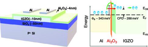
Although insertion of a thin insulating layer between metal electrodes and a semiconducting channel is an effective way to improve device performance, the exact reason for improvement in performance is not elucidated. Herein, the role of an Al2O3 interlayer sandwiched between Al metal electrodes and an amorphous indium–gallium–zinc–oxide semiconducting channel is systematically investigated. The Al2O3 interlayer results in not only a good transistor performance with increased on current but also improved gate bias stress stability. The improvement is primarily attributed to a doping effect and mitigation of interface defects. Energy‐band diagrams, experimentally obtained from temperature‐variable electrical characterization and electrostatic force microscopy, validate the channel doping effect, which increase the tunneling probability of the electron charge carriers via a reduction of the Schottky barrier width. A comprehensive study on the influence of various processing parameters, including Al2O3 thickness, post‐annealing treatment conditions, and types of electrodes, on the transistor device is also performed. This approach guides the practical implementation of stable sol–gel oxide‐based thin‐film transistors and promotes integrated circuitry applications.
中文翻译:

揭示了Al2O3中间层在铟镓锌氧化物晶体管中的作用
尽管在金属电极和半导体沟道之间插入薄绝缘层是提高器件性能的有效方法,但仍未阐明提高性能的确切原因。在此,系统地研究了夹在Al金属电极和非晶铟-镓-锌-氧化物半导体通道之间的Al 2 O 3中间层的作用。铝2 O 3中间层不仅在导通电流增加的情况下产生良好的晶体管性能,而且还改善了栅极偏置应力的稳定性。改善主要归因于掺杂效应和界面缺陷的减轻。从温度可变电特性和静电力显微镜实验获得的能带图验证了沟道掺杂效应,该沟道掺杂效应通过减小肖特基势垒宽度来增加电子载流子的隧穿概率。全面研究各种工艺参数(包括Al 2 O 3)的影响还可以在晶体管器件上执行厚度,退火后处理条件和电极类型的操作。这种方法指导了稳定的基于溶胶-氧化硅的薄膜晶体管的实际实施,并促进了集成电路的应用。
更新日期:2020-12-30
中文翻译:
揭示了Al2O3中间层在铟镓锌氧化物晶体管中的作用
尽管在金属电极和半导体沟道之间插入薄绝缘层是提高器件性能的有效方法,但仍未阐明提高性能的确切原因。在此,系统地研究了夹在Al金属电极和非晶铟-镓-锌-氧化物半导体通道之间的Al 2 O 3中间层的作用。铝2 O 3中间层不仅在导通电流增加的情况下产生良好的晶体管性能,而且还改善了栅极偏置应力的稳定性。改善主要归因于掺杂效应和界面缺陷的减轻。从温度可变电特性和静电力显微镜实验获得的能带图验证了沟道掺杂效应,该沟道掺杂效应通过减小肖特基势垒宽度来增加电子载流子的隧穿概率。全面研究各种工艺参数(包括Al 2 O 3)的影响还可以在晶体管器件上执行厚度,退火后处理条件和电极类型的操作。这种方法指导了稳定的基于溶胶-氧化硅的薄膜晶体管的实际实施,并促进了集成电路的应用。


 京公网安备 11010802027423号