当前位置:
X-MOL 学术
›
Phys. Status Solidi B
›
论文详情
Our official English website, www.x-mol.net, welcomes your feedback! (Note: you will need to create a separate account there.)
Change in Topography of InAs Submonolayer Nanostructures at the 2D to 3D Transition
Physica Status Solidi (B) - Basic Solid State Physics ( IF 1.6 ) Pub Date : 2020-12-07 , DOI: 10.1002/pssb.202000349 Ronel Christian Roca 1 , Itaru Kamiya 1
Physica Status Solidi (B) - Basic Solid State Physics ( IF 1.6 ) Pub Date : 2020-12-07 , DOI: 10.1002/pssb.202000349 Ronel Christian Roca 1 , Itaru Kamiya 1
Affiliation
|
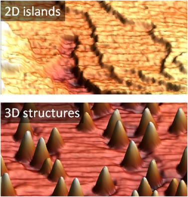
A strong topographical evidence of the 2D to 3D transition in InAs/GaAs nanostructures assembled by the submonolayer (SML) growth mode using molecular beam epitaxy (MBE) is reported. Whereas the 2D to 3D transition in InAs nanostructures assembled by the Stranski–Krastanov (SK) growth mode is well established with a critical thickness of around 1.7 monolayer (ML), the analogous phenomenon in SML‐grown nanostructures is not yet well understood. Herein, atomic force microscopy (AFM) is utilized to investigate the topographical changes associated with the 2D to 3D transition in SML nanostructures, and it is unambiguously shown that for a given number of stacks and GaAs matrix (spacer) layer thickness, there exists a critical thickness in the amount of deposited InAs per cycle, beyond which the nucleation of 3D nanostructures abruptly begins. It is also shown that the critical thickness decreases with increasing number of stacks as well as with decreasing GaAs matrix layer thickness. Moreover, the present work shows that InAs/GaAs SML nanostructures exist in two distinct forms: 2D wetting layer (WL)‐like islands and 3D quantum dot (QD)‐like structures.
中文翻译:

InAs亚单层纳米结构在2D到3D过渡时的形貌变化
有强烈的地形证据表明,使用分子束外延(MBE)通过亚单层(SML)生长模式组装的InAs / GaAs纳米结构中的2D到3D过渡。尽管由Stranski-Krastanov(SK)生长模式组装的InAs纳米结构中的2D到3D过渡已经很好地建立,其临界厚度约为1.7单层(ML),但尚未很好地理解SML生长的纳米结构中的类似现象。本文中,原子力显微镜(AFM)用于研究与SML纳米结构中2D到3D跃迁相关的形貌变化,并且明确地表明,对于给定数量的堆叠和GaAs基质(间隔层)层厚度,存在一个在每个循环中沉积的InAs量达到临界厚度后,3D纳米结构的成核突然开始。还表明,临界厚度随着堆叠数量的增加以及GaAs基体层厚度的减小而减小。此外,目前的工作表明InAs / GaAs SML纳米结构以两种不同的形式存在:2D润湿层(WL)状岛和3D量子点(QD)状结构。
更新日期:2021-02-09
中文翻译:
InAs亚单层纳米结构在2D到3D过渡时的形貌变化
有强烈的地形证据表明,使用分子束外延(MBE)通过亚单层(SML)生长模式组装的InAs / GaAs纳米结构中的2D到3D过渡。尽管由Stranski-Krastanov(SK)生长模式组装的InAs纳米结构中的2D到3D过渡已经很好地建立,其临界厚度约为1.7单层(ML),但尚未很好地理解SML生长的纳米结构中的类似现象。本文中,原子力显微镜(AFM)用于研究与SML纳米结构中2D到3D跃迁相关的形貌变化,并且明确地表明,对于给定数量的堆叠和GaAs基质(间隔层)层厚度,存在一个在每个循环中沉积的InAs量达到临界厚度后,3D纳米结构的成核突然开始。还表明,临界厚度随着堆叠数量的增加以及GaAs基体层厚度的减小而减小。此外,目前的工作表明InAs / GaAs SML纳米结构以两种不同的形式存在:2D润湿层(WL)状岛和3D量子点(QD)状结构。


 京公网安备 11010802027423号