当前位置:
X-MOL 学术
›
Appl. Surf. Sci.
›
论文详情
Our official English website, www.x-mol.net, welcomes your feedback! (Note: you will need to create a separate account there.)
GaAs Layer on c-plane Sapphire for Light Emitting Sources
Applied Surface Science ( IF 6.7 ) Pub Date : 2021-03-01 , DOI: 10.1016/j.apsusc.2020.148554 Rahul Kumar , Samir K. Saha , Andrian Kuchuk , Yurii Maidaniuk , Fernando Maia de Oliveira , Qigeng Yan , Mourad Benamara , Yuriy I. Mazur , Shui-Qing Yu , Gregory J. Salamo
Applied Surface Science ( IF 6.7 ) Pub Date : 2021-03-01 , DOI: 10.1016/j.apsusc.2020.148554 Rahul Kumar , Samir K. Saha , Andrian Kuchuk , Yurii Maidaniuk , Fernando Maia de Oliveira , Qigeng Yan , Mourad Benamara , Yuriy I. Mazur , Shui-Qing Yu , Gregory J. Salamo
|
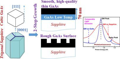
Abstract High-quality cubic GaAs (111)A buffer layers have been grown on an atomically flat c-plane trigonal sapphire substrate having well-defined steps and terraces. A two-step growth method has been used where, at an early stage, a GaAs layer has been grown at low temperature (LT), followed by second high-temperature GaAs growth layer. In addition to the two-step growth process, an AlAs nucleation layer and multiple annealing steps have been employed. The effectiveness of the LT GaAs layer in this highly dissimilar epitaxy was then investigated. An LT GaAs layer resulted in a relaxed GaAs buffer with smooth surface morphology and high crystalline quality. An InGaAs quantum well (QW) was epitaxially grown on the 70 nm GaAs buffer and compared with a reference InGaAs QW grown on a GaAs (111)A substrate. Along with x-ray and high-resolution cross-section transmission electron microscopy, comparable QW photoluminescence intensity and linewidth with respect to reference InGaAs QW confirmed the effectiveness of our growth strategies to produce high-quality GaAs on sapphire. This demonstrates the opportunity for GaAs photonics on sapphire and the potential to realise an integrated microwave photonic chip on a sapphire platform.
中文翻译:

用于发光源的 c 面蓝宝石上的 GaAs 层
摘要 高质量的立方 GaAs (111)A 缓冲层生长在原子级平坦的 c 面三角形蓝宝石衬底上,该衬底具有明确的台阶和台阶。已使用两步生长方法,其中在早期阶段,在低温 (LT) 下生长 GaAs 层,然后是第二个高温 GaAs 生长层。除了两步生长工艺外,还采用了 AlAs 成核层和多个退火步骤。然后研究了这种高度不同的外延中 LT GaAs 层的有效性。LT GaAs 层产生具有光滑表面形态和高结晶质量的松弛 GaAs 缓冲层。InGaAs 量子阱 (QW) 在 70 nm GaAs 缓冲器上外延生长,并与在 GaAs (111)A 衬底上生长的参考 InGaAs QW 进行比较。连同 X 射线和高分辨率横截面透射电子显微镜,与参考 InGaAs QW 相当的 QW 光致发光强度和线宽证实了我们的生长策略在蓝宝石上生产高质量 GaAs 的有效性。这展示了蓝宝石上 GaAs 光子学的机会,以及在蓝宝石平台上实现集成微波光子芯片的潜力。
更新日期:2021-03-01
中文翻译:
用于发光源的 c 面蓝宝石上的 GaAs 层
摘要 高质量的立方 GaAs (111)A 缓冲层生长在原子级平坦的 c 面三角形蓝宝石衬底上,该衬底具有明确的台阶和台阶。已使用两步生长方法,其中在早期阶段,在低温 (LT) 下生长 GaAs 层,然后是第二个高温 GaAs 生长层。除了两步生长工艺外,还采用了 AlAs 成核层和多个退火步骤。然后研究了这种高度不同的外延中 LT GaAs 层的有效性。LT GaAs 层产生具有光滑表面形态和高结晶质量的松弛 GaAs 缓冲层。InGaAs 量子阱 (QW) 在 70 nm GaAs 缓冲器上外延生长,并与在 GaAs (111)A 衬底上生长的参考 InGaAs QW 进行比较。连同 X 射线和高分辨率横截面透射电子显微镜,与参考 InGaAs QW 相当的 QW 光致发光强度和线宽证实了我们的生长策略在蓝宝石上生产高质量 GaAs 的有效性。这展示了蓝宝石上 GaAs 光子学的机会,以及在蓝宝石平台上实现集成微波光子芯片的潜力。


 京公网安备 11010802027423号