Our official English website, www.x-mol.net, welcomes your feedback! (Note: you will need to create a separate account there.)
Tailoring the transfer characteristics and hysteresis in MoS2 transistors using substrate engineering
Nanoscale ( IF 6.7 ) Pub Date : 2020-11-18 , DOI: 10.1039/d0nr05861k Pragya Prasad 1, 2, 3, 4 , Manjari Garg 1, 2, 3, 4 , U. Chandni 1, 2, 3, 4
Nanoscale ( IF 6.7 ) Pub Date : 2020-11-18 , DOI: 10.1039/d0nr05861k Pragya Prasad 1, 2, 3, 4 , Manjari Garg 1, 2, 3, 4 , U. Chandni 1, 2, 3, 4
Affiliation
|
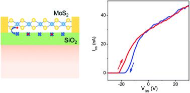
We demonstrate a novel form of transfer characteristics in substrate engineered MoS2 field effect transistors. Robust hysteresis with stable threshold voltages and a large gate voltage window is observed, which is suppressed at low temperatures. We analyse the dependence of the device characteristics on gate voltage range, gate stressing and sweep rates. We infer that the hysteresis originates from artificially created charged traps near the MoS2-SiO2 interface. These charge traps act as long range Coulomb scatterers and are screened at high carrier densities. The hysteresis is strongly suppressed in measurements on wafers devoid of the substrate treatment, providing a new extrinsic route to carefully tune the transfer characteristics.
中文翻译:

使用基板工程设计MoS2晶体管的传输特性和磁滞
我们展示了衬底工程MoS 2场效应晶体管中传输特性的一种新型形式。观察到具有稳定的阈值电压和较大的栅极电压窗口的鲁棒滞后现象,在低温条件下可以抑制这种滞后现象。我们分析了器件特性对栅极电压范围,栅极应力和扫描速率的依赖性。我们推断,滞后现象是由MoS 2 -SiO 2界面附近的人工产生的电荷陷阱引起的。这些电荷陷阱充当远程库仑散射体,并在高载流子密度下进行筛选。在没有进行基板处理的晶圆上的测量中,磁滞现象得到了极大的抑制,从而提供了一种新的外部途径来仔细调整传输特性。
更新日期:2020-11-25
中文翻译:
使用基板工程设计MoS2晶体管的传输特性和磁滞
我们展示了衬底工程MoS 2场效应晶体管中传输特性的一种新型形式。观察到具有稳定的阈值电压和较大的栅极电压窗口的鲁棒滞后现象,在低温条件下可以抑制这种滞后现象。我们分析了器件特性对栅极电压范围,栅极应力和扫描速率的依赖性。我们推断,滞后现象是由MoS 2 -SiO 2界面附近的人工产生的电荷陷阱引起的。这些电荷陷阱充当远程库仑散射体,并在高载流子密度下进行筛选。在没有进行基板处理的晶圆上的测量中,磁滞现象得到了极大的抑制,从而提供了一种新的外部途径来仔细调整传输特性。


 京公网安备 11010802027423号