当前位置:
X-MOL 学术
›
ACS Appl. Electron. Mater.
›
论文详情
Our official English website, www.x-mol.net, welcomes your feedback! (Note: you will need to create a separate account there.)
Resists for Helium Ion Beam Lithography: Recent Advances
ACS Applied Electronic Materials ( IF 4.7 ) Pub Date : 2020-11-24 , DOI: 10.1021/acsaelm.0c00627 Nagarjuna Ravi Kiran 1 , Manvendra Chauhan 2 , Satinder K. Sharma 2 , Subrata Ghosh 1 , Kenneth E. Gonsalves 1
ACS Applied Electronic Materials ( IF 4.7 ) Pub Date : 2020-11-24 , DOI: 10.1021/acsaelm.0c00627 Nagarjuna Ravi Kiran 1 , Manvendra Chauhan 2 , Satinder K. Sharma 2 , Subrata Ghosh 1 , Kenneth E. Gonsalves 1
Affiliation
|
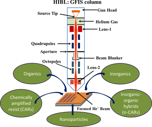
Since the fabrication of micro-/nanoelectronic devices are marching toward ultralow node technology with dense patterns to meet the current industry demands, continuous advancement is needed in terms of material design and lithographic techniques. In this perspective, helium ion beam lithography (HIBL) has gained tremendous attention of the scientific society to realize high-performance device fabrication with advanced technology. Salient features of the helium ion beam including sub-nanometer spot size, high-intensity lighter ion (with respect to gallium and neon ions) make the HIBL technique a competitive next-generation lithography tool. This review describes, in brief, the significance of HIBL technology in comparison with electron beam lithography (EBL); however, it presents in detail the development made in the area of resists for HIBL. One of the important characteristics of He+ beam is, reduced backscattering leads to minimizing the proximity effects in contrast with EBL. Furthermore, it emphasizes the developments of various resist materials to perform high-resolution patterns at comparable line-edge roughness/line-width roughness (LER/LWR) values. HIBL performances of various classes of materials are presented here to give a overall conception of the technique. The materials including organic, inorganic, organic–inorganic hybrids, and nanoscale materials which have shown promising patterning under He+ beam irradiation have been included and discussed in this work.
中文翻译:

抵抗氦离子束光刻技术的最新进展
由于微/纳米电子器件的制造正朝着具有致密图案的超低节点技术发展,以满足当前的工业需求,因此在材料设计和光刻技术方面需要不断发展。从这个角度来看,氦离子束光刻(HIBL)已获得科学界的极大关注,以利用先进技术实现高性能器件制造。氦离子束的显着特征包括亚纳米级的光点大小,高强度的轻离子(相对于镓和氖离子),使HIBL技术成为竞争性的下一代光刻工具。这篇综述简要地描述了HIBL技术与电子束光刻(EBL)相比的重要性。但是,它详细介绍了HIBL抗蚀剂领域的发展。+光束是,与EBL相比,减少的反向散射可最大程度地减小邻近效应。此外,它强调了各种抗蚀剂材料的发展,以在可比较的线边缘粗糙度/线宽粗糙度(LER / LWR)值下执行高分辨率图案。此处介绍了各种材料的HIBL性能,以全面介绍该技术。这项工作包括并讨论了包括有机,无机,有机-无机杂化材料和纳米级材料在内的材料,这些材料在He +束辐照下显示出有希望的图案。
更新日期:2020-12-22
中文翻译:
抵抗氦离子束光刻技术的最新进展
由于微/纳米电子器件的制造正朝着具有致密图案的超低节点技术发展,以满足当前的工业需求,因此在材料设计和光刻技术方面需要不断发展。从这个角度来看,氦离子束光刻(HIBL)已获得科学界的极大关注,以利用先进技术实现高性能器件制造。氦离子束的显着特征包括亚纳米级的光点大小,高强度的轻离子(相对于镓和氖离子),使HIBL技术成为竞争性的下一代光刻工具。这篇综述简要地描述了HIBL技术与电子束光刻(EBL)相比的重要性。但是,它详细介绍了HIBL抗蚀剂领域的发展。+光束是,与EBL相比,减少的反向散射可最大程度地减小邻近效应。此外,它强调了各种抗蚀剂材料的发展,以在可比较的线边缘粗糙度/线宽粗糙度(LER / LWR)值下执行高分辨率图案。此处介绍了各种材料的HIBL性能,以全面介绍该技术。这项工作包括并讨论了包括有机,无机,有机-无机杂化材料和纳米级材料在内的材料,这些材料在He +束辐照下显示出有希望的图案。


 京公网安备 11010802027423号