Our official English website, www.x-mol.net, welcomes your feedback! (Note: you will need to create a separate account there.)
Nanoscale Patterning of Carbon Nanotubes: Techniques, Applications, and Future
Advanced Science ( IF 15.1 ) Pub Date : 2020-11-23 , DOI: 10.1002/advs.202001778 Alexander Corletto 1 , Joseph G Shapter 1
Advanced Science ( IF 15.1 ) Pub Date : 2020-11-23 , DOI: 10.1002/advs.202001778 Alexander Corletto 1 , Joseph G Shapter 1
Affiliation
|
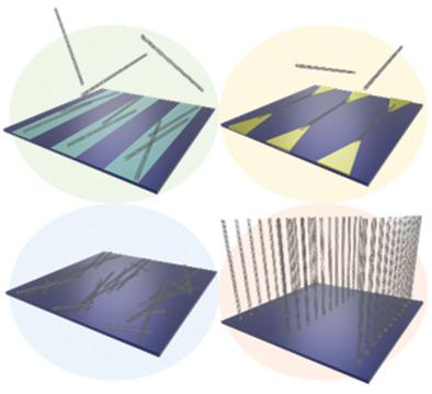
Carbon nanotube (CNT) devices and electronics are achieving maturity and directly competing or surpassing devices that use conventional materials. CNTs have demonstrated ballistic conduction, minimal scaling effects, high current capacity, low power requirements, and excellent optical/photonic properties; making them the ideal candidate for a new material to replace conventional materials in next‐generation electronic and photonic systems. CNTs also demonstrate high stability and flexibility, allowing them to be used in flexible, printable, and/or biocompatible electronics. However, a major challenge to fully commercialize these devices is the scalable placement of CNTs into desired micro/nanopatterns and architectures to translate the superior properties of CNTs into macroscale devices. Precise and high throughput patterning becomes increasingly difficult at nanoscale resolution, but it is essential to fully realize the benefits of CNTs. The relatively long, high aspect ratio structures of CNTs must be preserved to maintain their functionalities, consequently making them more difficult to pattern than conventional materials like metals and polymers. This review comprehensively explores the recent development of innovative CNT patterning techniques with nanoscale lateral resolution. Each technique is critically analyzed and applications for the nanoscale‐resolution approaches are demonstrated. Promising techniques and the challenges ahead for future devices and applications are discussed.
中文翻译:

碳纳米管的纳米级图案化:技术、应用和未来
碳纳米管(CNT)设备和电子产品正在走向成熟,并直接竞争或超越使用传统材料的设备。碳纳米管具有弹道传导、最小缩放效应、高电流容量、低功率要求以及优异的光学/光子特性;使它们成为替代下一代电子和光子系统中传统材料的新材料的理想候选者。碳纳米管还表现出高稳定性和灵活性,使其可用于柔性、可印刷和/或生物相容性电子产品。然而,这些器件完全商业化的一个主要挑战是将碳纳米管可扩展地放置到所需的微/纳米图案和架构中,以将碳纳米管的优越性能转化为宏观器件。在纳米级分辨率下进行精确、高通量的图案化变得越来越困难,但充分发挥碳纳米管的优势至关重要。必须保留碳纳米管相对较长、高纵横比的结构以维持其功能,因此使它们比金属和聚合物等传统材料更难图案化。本综述全面探讨了具有纳米级横向分辨率的创新碳纳米管图案化技术的最新发展。每种技术都经过严格分析,并演示了纳米级分辨率方法的应用。讨论了有前景的技术以及未来设备和应用面临的挑战。
更新日期:2021-01-07
中文翻译:
碳纳米管的纳米级图案化:技术、应用和未来
碳纳米管(CNT)设备和电子产品正在走向成熟,并直接竞争或超越使用传统材料的设备。碳纳米管具有弹道传导、最小缩放效应、高电流容量、低功率要求以及优异的光学/光子特性;使它们成为替代下一代电子和光子系统中传统材料的新材料的理想候选者。碳纳米管还表现出高稳定性和灵活性,使其可用于柔性、可印刷和/或生物相容性电子产品。然而,这些器件完全商业化的一个主要挑战是将碳纳米管可扩展地放置到所需的微/纳米图案和架构中,以将碳纳米管的优越性能转化为宏观器件。在纳米级分辨率下进行精确、高通量的图案化变得越来越困难,但充分发挥碳纳米管的优势至关重要。必须保留碳纳米管相对较长、高纵横比的结构以维持其功能,因此使它们比金属和聚合物等传统材料更难图案化。本综述全面探讨了具有纳米级横向分辨率的创新碳纳米管图案化技术的最新发展。每种技术都经过严格分析,并演示了纳米级分辨率方法的应用。讨论了有前景的技术以及未来设备和应用面临的挑战。


 京公网安备 11010802027423号