当前位置:
X-MOL 学术
›
Adv. Mater.
›
论文详情
Our official English website, www.x-mol.net, welcomes your feedback! (Note: you will need to create a separate account there.)
Indium Nitride at the 2D Limit
Advanced Materials ( IF 29.4 ) Pub Date : 2020-11-23 , DOI: 10.1002/adma.202006660 Béla Pécz 1 , Giuseppe Nicotra 2 , Filippo Giannazzo 2 , Rositsa Yakimova 3 , Antal Koos 1 , Anelia Kakanakova‐Georgieva 3
Advanced Materials ( IF 29.4 ) Pub Date : 2020-11-23 , DOI: 10.1002/adma.202006660 Béla Pécz 1 , Giuseppe Nicotra 2 , Filippo Giannazzo 2 , Rositsa Yakimova 3 , Antal Koos 1 , Anelia Kakanakova‐Georgieva 3
Affiliation
|
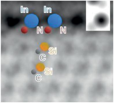
The properties of 2D InN are predicted to substantially differ from the bulk crystal. The predicted appealing properties relate to strong in‐ and out‐of‐plane excitons, high electron mobility, efficient strain engineering of their electronic and optical properties, and strong application potential in gas sensing. Until now, the realization of 2D InN remained elusive. In this work, the formation of 2D InN and measurements of its bandgap are reported. Bilayer InN is formed between graphene and SiC by an intercalation process in metal–organic chemical vapor deposition (MOCVD). The thickness uniformity of the intercalated structure is investigated by conductive atomic force microscopy (C‐AFM) and the structural properties by atomic resolution transmission electron microscopy (TEM). The coverage of the SiC surface is very high, above 90%, and a major part of the intercalated structure is represented by two sub‐layers of indium (In) bonded to nitrogen (N). Scanning tunneling spectroscopy (STS) measurements give a bandgap value of 2 ± 0.1 eV for the 2D InN. The stabilization of 2D InN with a pragmatic wide bandgap and high lateral uniformity of intercalation is demonstrated.
中文翻译:

二维极限氮化铟
预测2D InN的性质与块状晶体会有很大不同。预期的吸引人的特性涉及强平面内和平面激子,高电子迁移率,有效的电子和光学特性应变工程以及在气体传感中的强大应用潜力。到目前为止,2D InN的实现仍然遥遥无期。在这项工作中,报道了2D InN的形成及其带隙的测量。双层InN是通过金属有机化学气相沉积(MOCVD)中的插入过程在石墨烯和SiC之间形成的。通过导电原子力显微镜(C-AFM)研究插层结构的厚度均匀性,并通过原子分辨率透射电子显微镜(TEM)研究结构性能。SiC表面的覆盖率非常高,超过90%,插层结构的主要部分由与氮(N)结合的两个铟(In)子层代表。扫描隧道光谱(STS)测量得出2D InN的带隙值为2±0.1 eV。证明了具有实用的宽带隙和高横向均匀插层的2D InN的稳定性。
更新日期:2021-01-04
中文翻译:
二维极限氮化铟
预测2D InN的性质与块状晶体会有很大不同。预期的吸引人的特性涉及强平面内和平面激子,高电子迁移率,有效的电子和光学特性应变工程以及在气体传感中的强大应用潜力。到目前为止,2D InN的实现仍然遥遥无期。在这项工作中,报道了2D InN的形成及其带隙的测量。双层InN是通过金属有机化学气相沉积(MOCVD)中的插入过程在石墨烯和SiC之间形成的。通过导电原子力显微镜(C-AFM)研究插层结构的厚度均匀性,并通过原子分辨率透射电子显微镜(TEM)研究结构性能。SiC表面的覆盖率非常高,超过90%,插层结构的主要部分由与氮(N)结合的两个铟(In)子层代表。扫描隧道光谱(STS)测量得出2D InN的带隙值为2±0.1 eV。证明了具有实用的宽带隙和高横向均匀插层的2D InN的稳定性。


 京公网安备 11010802027423号