当前位置:
X-MOL 学术
›
Appl. Surf. Sci.
›
论文详情
Our official English website, www.x-mol.net, welcomes your feedback! (Note: you will need to create a separate account there.)
Properties of Nb3Sn films fabricated by magnetron sputtering from a single target
Applied Surface Science ( IF 6.7 ) Pub Date : 2021-03-01 , DOI: 10.1016/j.apsusc.2020.148528 Md Nizam Sayeed , Uttar Pudasaini , Charles E. Reece , Grigory V. Eremeev , Hani E. Elsayed-Ali
Applied Surface Science ( IF 6.7 ) Pub Date : 2021-03-01 , DOI: 10.1016/j.apsusc.2020.148528 Md Nizam Sayeed , Uttar Pudasaini , Charles E. Reece , Grigory V. Eremeev , Hani E. Elsayed-Ali
|
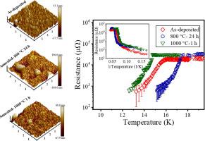
Abstract Superconducting Nb3Sn films were fabricated on sapphire and fine grain Nb substrates by magnetron sputtering from a single stoichiometric Nb3Sn target. The structural, morphological and superconducting properties of the films annealed for 24 h at temperatures of 800–1000 °C were investigated. The effect of the annealing time at 1000 °C was examined for 1, 12, and 24 h. The film properties were characterized by X-ray diffraction, scanning electron microscopy, atomic force microscopy, energy dispersive X-ray spectroscopy, and Raman spectroscopy. The DC superconducting properties of the films were characterized by a four-point probe measurement down to cryogenic temperatures. The RF surface resistance of films was measured over a temperature range of 6–23 K using a 7.4 GHz sapphire-loaded Nb cavity. As-deposited Nb3Sn films on sapphire had a superconducting critical temperature of 17.21 K, which improved to 17.83 K when the film was annealed at 800 °C for 24 h. For the films annealed at 1000 °C, the surface Sn content was reduced to ~11.3% for an annealing time of 12 h and to ~4.1% for an annealing time of 24 h. The Raman spectra of the films confirmed the microstructural evolution after annealing. The RF superconducting critical temperature of the as-deposited Nb3Sn films on Nb was 16.02 K, which increased to 17.44 K when the film was annealed at 800 °C for 24 h.
中文翻译:

单靶磁控溅射制备Nb3Sn薄膜的性能
摘要 在蓝宝石和细晶粒 Nb 衬底上通过磁控溅射从单个化学计量 Nb3Sn 靶材上制备了超导 Nb3Sn 薄膜。研究了在 800-1000°C 的温度下退火 24 小时的薄膜的结构、形态和超导性能。检查了 1000 °C 退火时间的影响,分别为 1、12 和 24 小时。通过X射线衍射、扫描电子显微镜、原子力显微镜、能量色散X射线光谱和拉曼光谱对薄膜特性进行表征。薄膜的直流超导特性通过低至低温的四点探针测量来表征。使用 7.4 GHz 蓝宝石负载 Nb 腔在 6-23 K 的温度范围内测量薄膜的 RF 表面电阻。蓝宝石上沉积的 Nb3Sn 薄膜的超导临界温度为 17.21 K,当薄膜在 800 °C 下退火 24 小时时,该温度提高到 17.83 K。对于在 1000 °C 下退火的薄膜,表面 Sn 含量在 12 小时的退火时间内降低到~11.3%,在退火时间为 24 小时时降低到~4.1%。薄膜的拉曼光谱证实了退火后的微观结构演变。Nb 上沉积的 Nb3Sn 薄膜的射频超导临界温度为 16.02 K,当薄膜在 800 °C 下退火 24 小时时,该温度增加到 17.44 K。薄膜的拉曼光谱证实了退火后的微观结构演变。Nb 上沉积的 Nb3Sn 薄膜的射频超导临界温度为 16.02 K,当薄膜在 800 °C 下退火 24 小时时,该温度增加到 17.44 K。薄膜的拉曼光谱证实了退火后的微观结构演变。Nb 上沉积的 Nb3Sn 薄膜的射频超导临界温度为 16.02 K,当薄膜在 800 °C 下退火 24 小时时,该温度增加到 17.44 K。
更新日期:2021-03-01
中文翻译:
单靶磁控溅射制备Nb3Sn薄膜的性能
摘要 在蓝宝石和细晶粒 Nb 衬底上通过磁控溅射从单个化学计量 Nb3Sn 靶材上制备了超导 Nb3Sn 薄膜。研究了在 800-1000°C 的温度下退火 24 小时的薄膜的结构、形态和超导性能。检查了 1000 °C 退火时间的影响,分别为 1、12 和 24 小时。通过X射线衍射、扫描电子显微镜、原子力显微镜、能量色散X射线光谱和拉曼光谱对薄膜特性进行表征。薄膜的直流超导特性通过低至低温的四点探针测量来表征。使用 7.4 GHz 蓝宝石负载 Nb 腔在 6-23 K 的温度范围内测量薄膜的 RF 表面电阻。蓝宝石上沉积的 Nb3Sn 薄膜的超导临界温度为 17.21 K,当薄膜在 800 °C 下退火 24 小时时,该温度提高到 17.83 K。对于在 1000 °C 下退火的薄膜,表面 Sn 含量在 12 小时的退火时间内降低到~11.3%,在退火时间为 24 小时时降低到~4.1%。薄膜的拉曼光谱证实了退火后的微观结构演变。Nb 上沉积的 Nb3Sn 薄膜的射频超导临界温度为 16.02 K,当薄膜在 800 °C 下退火 24 小时时,该温度增加到 17.44 K。薄膜的拉曼光谱证实了退火后的微观结构演变。Nb 上沉积的 Nb3Sn 薄膜的射频超导临界温度为 16.02 K,当薄膜在 800 °C 下退火 24 小时时,该温度增加到 17.44 K。薄膜的拉曼光谱证实了退火后的微观结构演变。Nb 上沉积的 Nb3Sn 薄膜的射频超导临界温度为 16.02 K,当薄膜在 800 °C 下退火 24 小时时,该温度增加到 17.44 K。


 京公网安备 11010802027423号