Our official English website, www.x-mol.net, welcomes your feedback! (Note: you will need to create a separate account there.)
Printed carbon nanotube thin-film transistors: progress on printable materials and the path to applications
Nanoscale ( IF 6.7 ) Pub Date : 2020-11-20 , DOI: 10.1039/d0nr06231f Shiheng Lu 1, 2, 3, 4 , Aaron D. Franklin 1, 2, 3, 4, 5
Nanoscale ( IF 6.7 ) Pub Date : 2020-11-20 , DOI: 10.1039/d0nr06231f Shiheng Lu 1, 2, 3, 4 , Aaron D. Franklin 1, 2, 3, 4, 5
Affiliation
|
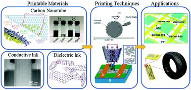
Printing technologies have attracted significant attention owing to their potential use in the low-cost manufacturing of custom or large-area flexible electronics. Among the many printable electronic materials that have been explored, semiconducting carbon nanotubes (CNTs) have shown increasing promise based on their exceptional electrical and mechanical properties, relative stability in air, and compatibility with several printing techniques to form semiconducting thin films. These attractive attributes make printed CNT thin films promising for applications including, but not limited to, sensors and display backplanes – at the heart of which is electronics’ most versatile device: the transistor. In this review, we present a summary of recent advancements in the field of printed carbon nanotube thin-film transistors (CNT-TFTs). In addition to an introduction of different printing techniques, together with their strengths and limitations, we discuss key aspects of ink/material selection and processing of various device components, including the CNT channels, contacts, and gate insulators. It is clear that printed CNT-TFTs are rapidly advancing, but there remain challenges, which are discussed along with current techniques to resolve them and future developments towards practical applications from these devices. There has been interest in low-cost, printable transistors for many years and the CNT-TFTs show great promise for delivering, but will not become a reality without further research advancement.
中文翻译:

印刷碳纳米管薄膜晶体管:可印刷材料的发展和应用途径
印刷技术由于其在低成本制造定制或大面积柔性电子产品中的潜在用途而备受关注。在已探索的许多可印刷电子材料中,半导体碳纳米管(CNT)由于其出色的电气和机械性能,在空气中的相对稳定性以及与形成半导体薄膜的几种印刷技术的兼容性而显示出越来越高的希望。这些吸引人的特性使印刷的CNT薄膜有望用于包括但不限于传感器和显示器背板的应用中-其核心是电子产品最通用的设备:晶体管。在这篇综述中,我们总结了印刷碳纳米管薄膜晶体管(CNT-TFT)领域的最新进展。除了介绍不同的印刷技术及其优点和局限性之外,我们还将讨论油墨/材料选择以及各种设备组件(包括CNT通道,触点和栅极绝缘体)的处理的关键方面。显然,印刷的CNT-TFT正在迅速发展,但是仍然存在挑战,这些挑战与解决这些问题的当前技术以及这些设备向实际应用的未来发展一起进行了讨论。多年来,人们一直对低成本,可印刷晶体管产生兴趣,并且CNT-TFT显示出了巨大的交付前景,但如果没有进一步的研究进展,它将不会成为现实。我们讨论了墨水/材料选择以及各种设备组件处理的关键方面,包括CNT通道,触点和栅极绝缘体。显然,印刷的CNT-TFT正在迅速发展,但是仍然存在挑战,这些挑战与解决这些问题的当前技术以及这些设备向实际应用的未来发展一起进行了讨论。多年来,人们一直对低成本,可印刷晶体管产生兴趣,并且CNT-TFT显示出了巨大的交付前景,但如果没有进一步的研究进展,它将不会成为现实。我们讨论了墨水/材料选择以及各种设备组件处理的关键方面,包括CNT通道,触点和栅极绝缘体。显然,印刷的CNT-TFT正在迅速发展,但是仍然存在挑战,这些挑战与解决这些问题的当前技术以及这些设备向实际应用的未来发展一起进行了讨论。多年来,人们一直对低成本,可印刷晶体管产生兴趣,并且CNT-TFT显示出了巨大的交付前景,但如果没有进一步的研究进展,它将不会成为现实。与解决这些问题的当前技术以及这些设备在实际应用中的未来发展一起进行了讨论。多年来,人们一直对低成本,可印刷晶体管产生兴趣,并且CNT-TFT显示出了巨大的交付前景,但如果没有进一步的研究进展,它将不会成为现实。与解决这些问题的当前技术以及这些设备在实际应用中的未来发展一起进行了讨论。多年来,人们一直对低成本,可印刷晶体管产生兴趣,并且CNT-TFT显示出了巨大的交付前景,但如果没有进一步的研究进展,它将不会成为现实。
更新日期:2020-11-21
中文翻译:
印刷碳纳米管薄膜晶体管:可印刷材料的发展和应用途径
印刷技术由于其在低成本制造定制或大面积柔性电子产品中的潜在用途而备受关注。在已探索的许多可印刷电子材料中,半导体碳纳米管(CNT)由于其出色的电气和机械性能,在空气中的相对稳定性以及与形成半导体薄膜的几种印刷技术的兼容性而显示出越来越高的希望。这些吸引人的特性使印刷的CNT薄膜有望用于包括但不限于传感器和显示器背板的应用中-其核心是电子产品最通用的设备:晶体管。在这篇综述中,我们总结了印刷碳纳米管薄膜晶体管(CNT-TFT)领域的最新进展。除了介绍不同的印刷技术及其优点和局限性之外,我们还将讨论油墨/材料选择以及各种设备组件(包括CNT通道,触点和栅极绝缘体)的处理的关键方面。显然,印刷的CNT-TFT正在迅速发展,但是仍然存在挑战,这些挑战与解决这些问题的当前技术以及这些设备向实际应用的未来发展一起进行了讨论。多年来,人们一直对低成本,可印刷晶体管产生兴趣,并且CNT-TFT显示出了巨大的交付前景,但如果没有进一步的研究进展,它将不会成为现实。我们讨论了墨水/材料选择以及各种设备组件处理的关键方面,包括CNT通道,触点和栅极绝缘体。显然,印刷的CNT-TFT正在迅速发展,但是仍然存在挑战,这些挑战与解决这些问题的当前技术以及这些设备向实际应用的未来发展一起进行了讨论。多年来,人们一直对低成本,可印刷晶体管产生兴趣,并且CNT-TFT显示出了巨大的交付前景,但如果没有进一步的研究进展,它将不会成为现实。我们讨论了墨水/材料选择以及各种设备组件处理的关键方面,包括CNT通道,触点和栅极绝缘体。显然,印刷的CNT-TFT正在迅速发展,但是仍然存在挑战,这些挑战与解决这些问题的当前技术以及这些设备向实际应用的未来发展一起进行了讨论。多年来,人们一直对低成本,可印刷晶体管产生兴趣,并且CNT-TFT显示出了巨大的交付前景,但如果没有进一步的研究进展,它将不会成为现实。与解决这些问题的当前技术以及这些设备在实际应用中的未来发展一起进行了讨论。多年来,人们一直对低成本,可印刷晶体管产生兴趣,并且CNT-TFT显示出了巨大的交付前景,但如果没有进一步的研究进展,它将不会成为现实。与解决这些问题的当前技术以及这些设备在实际应用中的未来发展一起进行了讨论。多年来,人们一直对低成本,可印刷晶体管产生兴趣,并且CNT-TFT显示出了巨大的交付前景,但如果没有进一步的研究进展,它将不会成为现实。


 京公网安备 11010802027423号