当前位置:
X-MOL 学术
›
Adv. Mater. Interfaces
›
论文详情
Our official English website, www.x-mol.net, welcomes your feedback! (Note: you will need to create a separate account there.)
Electrochemical Epitaxial Grown PbS Nanorods Array on Graphene Film for High‐Performance Photodetector
Advanced Materials Interfaces ( IF 5.4 ) Pub Date : 2020-11-16 , DOI: 10.1002/admi.202001464 Chan Yang 1 , Shuanglong Feng 1 , Linlong Tang 1 , Jun Shen 1 , Xingzhan Wei 1 , Haofei Shi 1
Advanced Materials Interfaces ( IF 5.4 ) Pub Date : 2020-11-16 , DOI: 10.1002/admi.202001464 Chan Yang 1 , Shuanglong Feng 1 , Linlong Tang 1 , Jun Shen 1 , Xingzhan Wei 1 , Haofei Shi 1
Affiliation
|
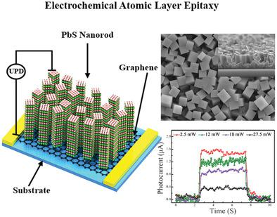
PbS based low dimensional heterostructures have shown promising IR photodetector applications, arising from the multiple exciton effect. However, owing to the difficulty in controlling the size, shape, nucleation, and growth of PbS nanorods, it remains a significant challenge to construct PbS nanorods array heterostructures with precisely controlled orientation, morphology, dimensionality, and spatial distribution of each component. Here, an electrochemical atomic layer epitaxial growth method is reported to prepare the PbS nanorods array‐graphene heterostructures by engineering the structures, sizes, dimensionalities, and morphologies lattice parameters of PbS. In these heterostructures, PbS nanorods selectively grow along (200) orientation on graphene film by adjusting the underpotential deposition. The high‐oriented PbS nanorods‐graphene heterostructure's growth dynamics are confirmed by comparing the extreme polarization of graphene, resulting in controllable growth orientation and nucleation. Furthermore, the PbS nanorods‐graphene heterostructure photodetector presents an extraordinary photoresponsivity in exceeding 10.4 A W−1 and figure‐of‐merit detection D* ≈ 2.98 × 10⁹ Jones is demonstrated in 2.7 µm at room temperature. The selective epitaxial growth of PbS nanorods opens the way to synthesize different hierarchical heterostructures with tunable architectures and dimensionalities, which can process various promising applications.
中文翻译:

高性能石墨烯薄膜上电化学外延生长的PbS纳米棒阵列
基于PbS的低维异质结构已显示出有希望的红外光电探测器应用,这是由于多重激子效应引起的。然而,由于难以控制PbS纳米棒的尺寸,形状,成核和生长,构建具有精确控制的各个组分的取向,形态,尺寸和空间分布的PbS纳米棒阵列异质结构仍然是一项重大挑战。在这里,据报道,通过对PbS的结构,尺寸,尺寸和形态晶格参数进行工程设计,电化学原子层外延生长方法可以制备PbS纳米棒阵列-石墨烯异质结构。在这些异质结构中,PbS纳米棒通过调节欠电位沉积在石墨烯薄膜上沿(200)取向选择性生长。通过比较石墨烯的极端极化,可以确认高取向的PbS纳米棒-石墨烯异质结构的生长动力学,从而可控制生长取向和成核。此外,PbS纳米棒-石墨烯异质结构光电探测器在超过10.4 AW时表现出非凡的光响应性-1和品质因数检测D *≈2.98×10 9 Jones在室温下以2.7 µm演示。PbS纳米棒的选择性外延生长为合成具有可调结构和尺寸的不同层次异质结构开辟了道路,该结构可以处理各种有前途的应用。
更新日期:2021-01-12
中文翻译:
高性能石墨烯薄膜上电化学外延生长的PbS纳米棒阵列
基于PbS的低维异质结构已显示出有希望的红外光电探测器应用,这是由于多重激子效应引起的。然而,由于难以控制PbS纳米棒的尺寸,形状,成核和生长,构建具有精确控制的各个组分的取向,形态,尺寸和空间分布的PbS纳米棒阵列异质结构仍然是一项重大挑战。在这里,据报道,通过对PbS的结构,尺寸,尺寸和形态晶格参数进行工程设计,电化学原子层外延生长方法可以制备PbS纳米棒阵列-石墨烯异质结构。在这些异质结构中,PbS纳米棒通过调节欠电位沉积在石墨烯薄膜上沿(200)取向选择性生长。通过比较石墨烯的极端极化,可以确认高取向的PbS纳米棒-石墨烯异质结构的生长动力学,从而可控制生长取向和成核。此外,PbS纳米棒-石墨烯异质结构光电探测器在超过10.4 AW时表现出非凡的光响应性-1和品质因数检测D *≈2.98×10 9 Jones在室温下以2.7 µm演示。PbS纳米棒的选择性外延生长为合成具有可调结构和尺寸的不同层次异质结构开辟了道路,该结构可以处理各种有前途的应用。


 京公网安备 11010802027423号