Microelectronics Journal ( IF 2.2 ) Pub Date : 2020-11-13 , DOI: 10.1016/j.mejo.2020.104944 Jalil Mazloum , Samad Sheikhaei
|
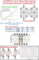
In this paper, a novel passive super–harmonic coupling QVCO is presented. The coupling is achieved by Cross–Connecting the top and bottom Common–Source nodes in the complementary (current reuse) LC Cross–Coupled oscillator topology, and therefore, the circuit is named as C3S–QVCO. Unlike the transformer coupling QVCO (TC–QVCO), as the typical super–harmonic coupling technique, the die area is not increased. Also, in the proposed QVCO, neither additional power consumption nor additional noise generator component is required, for quadrature operation. Therefore, the proposed QVCO has a good power consumption performance. The proposed method is evaluated theoretically and analytically, and it is proved that the proposed method is capable of generating multi–phase outputs. The proposed QVCO is designed in a 0.18 μm RF–CMOS technology with a power supply of 1.8 V, the current consumption of 6.25 mA, and the tuning range of 3.75–3.95 GHz (5.3%). Post layout simulation result shows −129 dBc/Hz, and 190 dB phase noise and FOM for the proposed QVCO at 1 MHz offset from the 3.75 GHz frequency. The proposed QVCO presents 6 dB phase noise improvement compared to parallel (P)–QVCO and also demonstrates similar phase noise performance to that of the TC–QVCO, with the same power consumption. Maximum phase/amplitude errors of the proposed QVCO for a 1% mismatch in the oscillator’s tank capacitors are 0.72°/2 mV, in the whole tuning range. Those are 0.77°/7.3 mV for the P–QVCO and 1.3°/2.3 mV for the TC–QVCO.
中文翻译:
C3S–QVCO:具有交叉连接的共源节点的低相位噪声,低功耗,超谐波耦合QVCO
在本文中,提出了一种新颖的无源超谐波耦合QVCO。通过交叉连接互补(电流重用)LC交叉耦合振荡器拓扑中的顶部和底部公共源节点来实现耦合,因此该电路被命名为C3S–QVCO。与变压器耦合QVCO(TC–QVCO)不同,作为典型的超谐波耦合技术,芯片面积不会增加。同样,在提出的QVCO中,对于正交操作,不需要额外的功耗或额外的噪声发生器组件。因此,所提出的QVCO具有良好的功耗性能。对所提方法进行了理论和分析评价,证明了所提方法能够产生多相输出。建议的QVCO设计为0。18μmRF-CMOS技术,电源电压为1.8 V,电流消耗为6.25 mA,调谐范围为3.75-3.95 GHz(5.3%)。布局后的仿真结果显示,与3.75 GHz频率偏移1 MHz时,拟议QVCO的−129 dBc / Hz,190 dB的相位噪声和FOM。与并联(P)–QVCO相比,拟议的QVCO提出了6 dB的相位噪声改善,并且在相同功耗的情况下,还证明了与TC–QVCO相似的相位噪声性能。在整个调谐范围内,对于振荡器的储能电容失配1%的拟议QVCO的最大相位/幅度误差为0.72°/ 2 mV。对于P–QVCO,这些为0.77°/ 7.3 mV;对于TC–QVCO,这些为1.3°/ 2.3 mV。拟议QVCO在距3.75 GHz频率1 MHz处的相位噪声和FOM为190 dB。与并联(P)–QVCO相比,拟议的QVCO提出了6 dB的相位噪声改善,并且在相同功耗的情况下,还证明了与TC–QVCO相似的相位噪声性能。在整个调谐范围内,对于振荡器的储能电容失配1%的拟议QVCO的最大相位/幅度误差为0.72°/ 2 mV。对于P–QVCO,这些为0.77°/ 7.3 mV;对于TC–QVCO,这些为1.3°/ 2.3 mV。拟议QVCO在距3.75 GHz频率1 MHz处的相位噪声和FOM为190 dB。与并联(P)–QVCO相比,拟议的QVCO提出了6 dB的相位噪声改善,并且在相同功耗的情况下,还证明了与TC–QVCO相似的相位噪声性能。在整个调谐范围内,对于振荡器的储能电容失配1%的拟议QVCO的最大相位/幅度误差为0.72°/ 2 mV。对于P–QVCO,这些为0.77°/ 7.3 mV;对于TC–QVCO,这些为1.3°/ 2.3 mV。在整个调谐范围内,对于振荡器的储能电容失配1%的拟议QVCO的最大相位/幅度误差为0.72°/ 2 mV。对于P–QVCO,这些为0.77°/ 7.3 mV;对于TC–QVCO,这些为1.3°/ 2.3 mV。在整个调谐范围内,对于振荡器的储能电容失配1%的拟议QVCO的最大相位/幅度误差为0.72°/ 2 mV。对于P–QVCO,这些为0.77°/ 7.3 mV;对于TC–QVCO,这些为1.3°/ 2.3 mV。


 京公网安备 11010802027423号