当前位置:
X-MOL 学术
›
ACS Appl. Nano Mater.
›
论文详情
Our official English website, www.x-mol.net, welcomes your feedback! (Note: you will need to create a separate account there.)
Peroxide-Induced Tuning of the Conductivity of Nanometer-Thick MoS2 Films for Solid-State Sensors
ACS Applied Nano Materials ( IF 5.9 ) Pub Date : 2020-11-06 , DOI: 10.1021/acsanm.0c02135 Dipankar Saha 1 , Ponnambalam Ravi Selvaganapathy 2 , Peter Kruse 1
ACS Applied Nano Materials ( IF 5.9 ) Pub Date : 2020-11-06 , DOI: 10.1021/acsanm.0c02135 Dipankar Saha 1 , Ponnambalam Ravi Selvaganapathy 2 , Peter Kruse 1
Affiliation
|
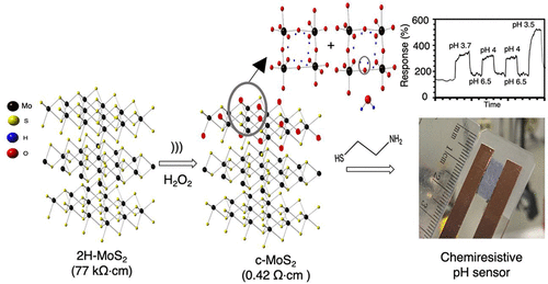
Applications of molybdenum disulfide (MoS2) in energy storage devices, solar cells, electrocatalysts, and sensors require good electrical conductivity. However, neither of the current ways to prepare conductive MoS2 (lithium intercalation and hydrothermal processes) is easily amenable to scale-up. A possible alternative pathway is the modulation of the electronic properties of the semiconducting form of MoS2 through structural defects. Here, we report the preparation of nanoscale conductive MoS2 flakes by treating exfoliated 2H-MoS2 with dilute aqueous hydrogen peroxide at room temperature. Sheet resistance measurements as well as Raman and photoelectron spectroscopy reveal the partial formation of hydrogen molybdenum bronze (HxMoO3) and substoichiometric MoO3–y, which help tune the conductivity of the nanometer-scale thin films without impacting the sulfur-to-molybdenum ratio. We have cast the material into thin film networks to fabricate highly stable chemiresistive pH sensors. Our work introduces a straightforward and safe way of preparing a conductive form of MoS2 and its application as a low-cost solid-state sensor.
中文翻译:

过氧化物诱导的用于固态传感器的纳米厚MoS 2薄膜电导率的调谐
二硫化钼(MoS 2)在储能设备,太阳能电池,电催化剂和传感器中的应用要求良好的导电性。但是,目前两种制备导电性MoS 2的方法(锂嵌入和水热工艺)都不容易按比例放大。可能的替代途径是通过结构缺陷调节MoS 2半导体形式的电子特性。在这里,我们报告通过处理脱落的2H-MoS 2制备纳米级导电MoS 2薄片在室温下用稀的过氧化氢水溶液洗涤。薄层电阻测量以及拉曼光谱和光电子能谱揭示了氢钼青铜(H x MoO 3)和亚化学计量的MoO 3– y的部分形成,这有助于调整纳米级薄膜的电导率,而不会影响硫磺制氢。钼比。我们已将材料浇铸成薄膜网络,以制造高度稳定的化学耐性pH传感器。我们的工作介绍了一种制备导电形式的MoS 2的简单而安全的方法,并将其用作低成本的固态传感器。
更新日期:2020-11-25
中文翻译:
过氧化物诱导的用于固态传感器的纳米厚MoS 2薄膜电导率的调谐
二硫化钼(MoS 2)在储能设备,太阳能电池,电催化剂和传感器中的应用要求良好的导电性。但是,目前两种制备导电性MoS 2的方法(锂嵌入和水热工艺)都不容易按比例放大。可能的替代途径是通过结构缺陷调节MoS 2半导体形式的电子特性。在这里,我们报告通过处理脱落的2H-MoS 2制备纳米级导电MoS 2薄片在室温下用稀的过氧化氢水溶液洗涤。薄层电阻测量以及拉曼光谱和光电子能谱揭示了氢钼青铜(H x MoO 3)和亚化学计量的MoO 3– y的部分形成,这有助于调整纳米级薄膜的电导率,而不会影响硫磺制氢。钼比。我们已将材料浇铸成薄膜网络,以制造高度稳定的化学耐性pH传感器。我们的工作介绍了一种制备导电形式的MoS 2的简单而安全的方法,并将其用作低成本的固态传感器。


 京公网安备 11010802027423号