当前位置:
X-MOL 学术
›
Adv. Opt. Mater.
›
论文详情
Our official English website, www.x-mol.net, welcomes your feedback! (Note: you will need to create a separate account there.)
Wafer‐Scale Fabrication of 2D β‐In2Se3 Photodetectors
Advanced Optical Materials ( IF 9 ) Pub Date : 2020-11-09 , DOI: 10.1002/adom.202001034 Marcel S. Claro 1, 2 , Justyna Grzonka 1 , Nicoleta Nicoara 1, 2 , Paulo J. Ferreira 1, 3, 4 , Sascha Sadewasser 1, 2
Advanced Optical Materials ( IF 9 ) Pub Date : 2020-11-09 , DOI: 10.1002/adom.202001034 Marcel S. Claro 1, 2 , Justyna Grzonka 1 , Nicoleta Nicoara 1, 2 , Paulo J. Ferreira 1, 3, 4 , Sascha Sadewasser 1, 2
Affiliation
|
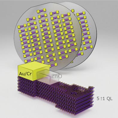
2D materials are considered the future of electronics and photonics, stimulated by their remarkable performance. Among the 2D materials family, β‐In2Se3 shows good mobility, excellent photoresponsivity, and exotic ferroelectricity, making it suitable for a wide variety of applications. To date, most reported devices from 2D materials in general, and β‐In2Se3 in specific, rely on cumbersome fabrication methods using mechanical exfoliation and transfer of layers onto other substrates. However, for a successful adoption of 2D materials in industry, reliable and reproducible large‐area growth of 2D materials is required. Here, the wafer‐scale epitaxial growth of 2D β‐In2Se3 on c‐sapphire using molecular beam epitaxy is demonstrated. Excellent materials quality of thick (90 nm) and very thin films, down to two quintuple layers (2 nm) is confirmed. Furthermore, the fabrication of hundreds of photodetector devices on a 2 in. wafer, using five quintuple layers of β‐In2Se3, is demonstrated. They are sensitive to near‐infrared light up to 898 nm wavelength and show a response time of ≈7 ms, which is faster than any result previously reported for β‐In2Se3 photodetectors. The devices are produced using photolithography and other standard semiconductor processing methods, which allows easy integration into the current Si technology.
中文翻译:

2Dβ-In2Se3光电探测器的晶圆级制造
二维材料因其出色的性能而被认为是电子和光子学的未来。间的2D材料家族,β-在2硒3示出良好的流动性,优异的光响应,和外来铁电性,使其适用于各种各样的应用。迄今为止,大多数报道的从2D材料的装置在一般情况下,和β-在2硒3中具体地,依赖于使用机械剥离和层的转移到其它底物繁琐的制造方法。但是,要成功地在工业中采用2D材料,就需要可靠且可重现的2D材料大面积增长。这里,2D的晶片规模外延生长β-在2硒3上证明了使用分子束外延的c蓝宝石。厚膜(90 nm)和非常薄的膜(低至两层五层(2 nm))的优异材料质量得到证实。此外,在2数百光电检测器部件的英寸晶片的制造中,使用五种五元组层β-在2硒3,是证明。它们对近红外光到898纳米的波长敏感,并显示≈7毫秒的响应时间,这是比以前β-在报告的任何结果更快2硒3光电检测器。该器件采用光刻技术和其他标准半导体加工方法生产,可轻松集成到当前的Si技术中。
更新日期:2021-01-04
中文翻译:
2Dβ-In2Se3光电探测器的晶圆级制造
二维材料因其出色的性能而被认为是电子和光子学的未来。间的2D材料家族,β-在2硒3示出良好的流动性,优异的光响应,和外来铁电性,使其适用于各种各样的应用。迄今为止,大多数报道的从2D材料的装置在一般情况下,和β-在2硒3中具体地,依赖于使用机械剥离和层的转移到其它底物繁琐的制造方法。但是,要成功地在工业中采用2D材料,就需要可靠且可重现的2D材料大面积增长。这里,2D的晶片规模外延生长β-在2硒3上证明了使用分子束外延的c蓝宝石。厚膜(90 nm)和非常薄的膜(低至两层五层(2 nm))的优异材料质量得到证实。此外,在2数百光电检测器部件的英寸晶片的制造中,使用五种五元组层β-在2硒3,是证明。它们对近红外光到898纳米的波长敏感,并显示≈7毫秒的响应时间,这是比以前β-在报告的任何结果更快2硒3光电检测器。该器件采用光刻技术和其他标准半导体加工方法生产,可轻松集成到当前的Si技术中。


 京公网安备 11010802027423号