Sensors and Actuators A: Physical ( IF 4.6 ) Pub Date : 2020-11-07 , DOI: 10.1016/j.sna.2020.112421 Tran Le , Huu Phuc Dang
|
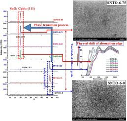
Herein, the hole concentration of a SnO2 film has been increased by the co-doping of Sb and N in the SnO2 host lattice. The N-substituted O content in the SnO2 lattice was observed to depend on the N2 gas percentage in a mixed sputtering gas (comprising Ar and N2) and the Sb-substituted Sn content in the host lattice. The N-substituted O content in the SnO2 lattice increased with N2 gas concentration in the mixed sputtering gas and the Sb2O3 content in the STO (Sb2O3- doped SnO2) target. An optimal number of N-substituted O and Sb-substituted Sn contents occurred for the target with 6 % wt. Sb2O3 and the mixed sputtering gas with 75 % N2, respectively, owing to the high electrical conductivity and the best crystal quality. N-substituted O and Sb-substituted Sn contents were detected using X-ray photoelectron spectroscopy, energy-dispersive X-ray spectroscopy, ultraviolet-visible spectroscopy, and XRD pattern measurements. The N-substituted O sites in the host lattice are large enough to cause the tetragonal rutile-to-cubic phase transformation. The film crystal quality of the cubic phase is higher than that of the rutile one. The lowest resistivity and the highest hole mobility were measured to be 1.0 × 10⁻² Ω cm and 4.26 cm2 V−1 s−1, respectively, corresponding to the hole concentration of 1.24 × 1020 cm−3. The electrical property and the crystal quality of p-type Sb- and N- co-doped SnO2 films were improved compared to Sb- or N- doped SnO2 films. The deposition temperature dropped 300 °C for Sb- or N- co-doped SnO2 film instead of 550 °C for Sb-doped SnO2 film. The I–V plots of SNTO-6-y/n-Si junctions under dark and light conditions corroborated that the conductive SNTO-6-y films are p-type. The results showed that the photocurrent for SNTO-6-75 diode achieves the highest value due to the high crystal quality and the low surface roughness of SNTO-6-75 film compared to the other films. The on-off photocurrent response confirmed the stable reproducibility of the SNTO-6-75 diode. The photo-electronic effect of p-type Sb- and N- co-doped SnO2 films is promising to apply for photodetector or the other optoelectronic devices.
中文翻译:
SnO 2晶格中的Sb含量和混合溅射气体中的N 2百分比对SnO 2膜中N溶解度的影响
在此,通过在SnO 2主晶格中Sb和N的共掺杂而增加了SnO 2膜的空穴浓度。观察到SnO 2晶格中的N-取代的O含量取决于混合溅射气体(包含Ar和N 2)中的N 2气体百分比和主体晶格中的Sb-取代的Sn含量。SnO 2晶格中的N-取代O含量随混合溅射气体中N 2气体浓度和STO(掺杂Sb 2 O 3的SnO 2)中的Sb 2 O 3含量而增加。)目标。对于具有6重量%的靶,出现了N-取代的O和Sb-取代的Sn含量的最佳数量。由于具有高的电导率和最佳的晶体质量,Sb 2 O 3和具有75%N 2的混合溅射气体。使用X射线光电子能谱,能量色散X射线能谱,紫外可见光谱和XRD图谱测量来检测N-取代的O和Sb-取代的Sn含量。主晶格中的N-取代的O位足够大,足以引起四方金红石-立方相转变。立方相的薄膜晶体质量高于金红石相。最低的电阻率和最高的空穴迁移率经测量为1.0×10 -2分别为Ωcm和4.26 cm 2 V -1 s -1,对应于1.24×10 20 cm -3的空穴浓度。与Sb或N掺杂的SnO 2薄膜相比,p型Sb和N掺杂的SnO 2薄膜的电性能和晶体质量得到了改善。对于Sb或N-共掺杂的SnO 2膜,沉积温度下降了300°C,而对于Sb掺杂的SnO 2膜,沉积温度下降了550°C 。SNTO-6- y / n-Si结在黑暗和明亮条件下的IV图证实了导电SNTO-6- y胶卷是p型的。结果表明,与其他薄膜相比,SNTO-6-75二极管的光电流由于具有较高的晶体质量和较低的表面粗糙度而达到了最大值。开-关光电流响应证实了SNTO-6-75二极管的稳定重现性。p型掺Sb和N的SnO 2薄膜的光电效应有望应用于光电探测器或其他光电器件。


 京公网安备 11010802027423号