Chemical Engineering Journal ( IF 15.1 ) Pub Date : 2020-11-05 , DOI: 10.1016/j.cej.2020.127644 Wanli Li , Lingying Li , Qingqing Sun , Xuying Liu , Masayuki Kanehara , Tomonobu Nakayama , Jinting Jiu , Kenji Sakamoto , Takeo Minari
|
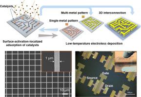
Patterning high-resolution multi-metal layers without using subtractive lithography poses a substantial challenge but is indispensable for the development of the modern electronics industry, especially flexible electronics. Herein, the general and feasible additive manufacturing approach is reported to selectively deposit high-resolution multi-metal patterns via surface-activation-localized electroless plating (SALEP) and enable the fabrication of 3-dimensional (3D) interconnections and high-performance organic thin-film transistor (OTFT) arrays for flexible electronics. The SALEP approach comprises the direct layer-by-layer deposition of multi-metal patterns interconnected by via holes, which are defined by the selective adsorption of palladium catalysts and a metallization process. The localized adsorption of the catalyst is guided by the difference in surface wettability and adsorbability caused by vacuum ultraviolet (VUV)-induced photochemical modification. The low-temperature and 3D approach enables miniaturization of flexible electrical circuits down to 1 µm in width; it also enables integration of an OTFT array on a flexible substrate. The fabricated OTFT array with multi-metal Cu/Ni/Au as contact electrodes exhibits a high hole mobility exceeding 10 cm2 V−1 s−1, demonstrating the adaptability of the SALEP approach for the low-cost, high-efficiency, and scalable fabrication of high-performance flexible electronic devices.
中文翻译:
通过表面活化局部化学镀直接制造高分辨率和高性能的柔性电子产品
在不使用减法光刻的情况下对高分辨率的多金属层进行图案化构成了巨大的挑战,但对于现代电子工业尤其是柔性电子工业的发展而言是必不可少的。在此,据报道,通用且可行的增材制造方法是通过表面活化局部化学镀(SALEP)选择性沉积高分辨率多金属图案,并能够制造3维(3D)互连和高性能有机薄膜柔性电子的薄膜晶体管(OTFT)阵列。SALEP方法包括通过通孔互连的多金属图案的直接逐层沉积,这由钯催化剂的选择性吸附和金属化过程定义。催化剂的局部吸附受真空紫外(VUV)诱导的光化学改性引起的表面润湿性和吸附性差异的影响。低温和3D方法使宽度小于1 µm的柔性电路小型化;它还可以在柔性基板上集成OTFT阵列。以多金属Cu / Ni / Au作为接触电极制成的OTFT阵列具有超过10 cm的高空穴迁移率2 V -1 s -1,证明了SALEP方法适用于低成本,高效率和可扩展的高性能柔性电子设备的制造。


 京公网安备 11010802027423号