Applied Materials Today ( IF 8.3 ) Pub Date : 2020-11-01 , DOI: 10.1016/j.apmt.2020.100858 Yonatan Calahorra , Bogdan Spiridon , Adina Wineman , Tommaso Busolo , Peter Griffin , Piotr K Szewczyk , Tongtong Zhu , Qingshen Jing , Rachel Oliver , Sohini Kar-Narayan
|
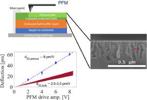
Electrical polarization phenomena in GaN are important as they have significant impact on the operation of modern day energy efficient lighting and are fundamental to GaN-based high power and high frequency electronics. Controlling polarization is beneficial for the optimization of these applications. GaN is also piezoelectric, and therefore mechanical stress and strain are possible handles to control its polarization. Nonetheless, polar semiconductors in general, and GaN in particular, are weak piezoelectric materials when compared to ceramics, and are therefore not considered for characteristic electromechanical applications such as sensing, actuation and mechanical energy harvesting. Here, we examine the effect of nanoscale porosity on the piezoelectricity of initially conductive GaN. We find that for 40% porosity, the previously conductive GaN layer becomes depleted, and exhibits enhanced piezoelectricity as measured using piezoresponse force microscopy, as well as by using a mechanical energy harvesting setup. The effective piezoelectric charge coefficient of the porous GaN, d33,eff, is found to be about 8 pm/V which is 2-3 times larger than bulk GaN. A macroscale device comprising a porous GaN layer delivered 100 nW/cm2 across a resistive load under a 150 kPa mechanical excitation. We performed finite element simulations to analyze the evolution of the piezoelectric properties with porosity. The simulations suggest that increased mechanical compliance due to porosity gives rise to the observed enhanced piezoelectricity in GaN. Furthermore, the simulations show that for stress-based excitations, the porous GaN electromechanical figure of merit is increased by an order of magnitude and becomes comparable to that of barium titanate piezoceramics. In addition, considering the central role played by GaN in modern electronics and optoelectronics, our study validates a very promising research direction when considering stress-based electromechanical applications which combine GaN's semiconducting and piezoelectric properties.
中文翻译:
纳米级孔隙率提高了半导体GaN的压电性和机电效率
GaN中的电极化现象非常重要,因为它们会对现代节能照明的运行产生重大影响,并且是基于GaN的大功率和高频电子设备的基础。控制极化有利于优化这些应用。GaN也是压电的,因此可以通过机械应力和应变来控制其极化。尽管如此,与陶瓷相比,极性半导体(尤其是GaN)通常是较弱的压电材料,因此不被考虑用于特征性的机电应用,例如传感,驱动和机械能收集。在这里,我们研究了纳米级孔隙率对初始导电GaN压电性的影响。我们发现孔隙率为40%先前的导电GaN层将耗尽,并显示出更高的压电性,如使用压电响应力显微镜以及使用机械能采集装置所测量的。多孔GaN的有效压电电荷系数发现d 33,eff约为8 pm / V,是体GaN的2-3倍。包括递送为100 nW / cm 2的多孔GaN层的宏观器件在150 kPa机械激励下跨越电阻性负载。我们进行了有限元模拟,以分析压电性能随孔隙率的变化。该模拟表明,由于孔隙率而导致的机械柔韧性提高,导致所观察到的GaN压电性增强。此外,仿真表明,对于基于应力的激励,多孔GaN机电性能因数提高了一个数量级,并且可以与钛酸钡压电陶瓷相媲美。此外,考虑到GaN在现代电子学和光电学中的核心作用,我们的研究验证了在考虑将GaN的半导体和压电特性相结合的基于应力的机电应用中非常有前途的研究方向。


 京公网安备 11010802027423号