International Journal of Machine Tools and Manufacture ( IF 14.0 ) Pub Date : 2020-10-26 , DOI: 10.1016/j.ijmachtools.2020.103649 Zhidong Fang , Yi Zhang , Rulin Li , Yanan Liang , Hui Deng
|
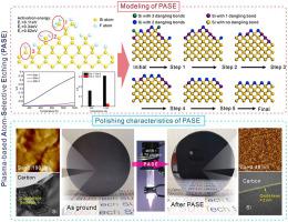
To realize the damage-free, highly efficient, and atomic-level polishing of single-crystal Si, plasma-based atom-selective etching (PASE) is proposed in this study as a generic polishing approach for Si wafers. The polishing effect of PASE is realized through the selective removal of Si atoms with more dangling bonds under high temperature. Plasma diagnostics are carried out to investigate the radical composition, the density of plasma, and the etching temperature. The key parameters of PASE are optimized, and the PASE of Si (100) with a material removal rate greater than 0.7 μm/min was realized. A ground Si (100) surface can be quickly smoothed by PASE, with the Sa roughness being reduced from 195 nm to below 1.0 nm within 5 min, and the polished surface is proven to be crystallographically perfect. The PASE of (110)- and (111)-oriented Si wafers is also proven effective, demonstrating that PASE is a generic polishing approach for Si regardless of orientation. The entire surface flattening of a 2-inch Si wafer was carried out by numerically controlled PASE, and the wafer flatness was reduced from 37.29 μm to 4.92 μm through optimized scanning conditions. Overall, this study has shown that PASE is a promising approach for high-efficiency and high-quality polishing of Si.
中文翻译:
通过基于等离子体的原子选择性蚀刻对单晶硅进行原子级抛光的有效方法
为了实现单晶硅的无损,高效和原子级抛光,本研究提出了基于等离子体的原子选择性蚀刻(PASE)作为硅晶片的通用抛光方法。PASE的抛光效果是通过在高温下选择性去除带有更多悬空键的Si原子来实现的。进行等离子体诊断以研究自由基的组成,等离子体的密度和蚀刻温度。优化了PASE的关键参数,实现了材料去除速率大于0.7μm/ min的Si(100)的PASE。通过PASE可以快速抛光Si(100)表面,并在5分钟内将Sa粗糙度从195 nm降低到1.0 nm以下,并且抛光后的表面在晶体学上被证明是完美的。还证明了(110)和(111)取向的Si晶片的PASE有效,这表明PASE是与Si无关的通用抛光方法。通过数控PASE对2英寸Si晶片的整个表面进行平坦化处理,并通过优化的扫描条件将晶片的平坦度从37.29μm降低到4.92μm。总体而言,这项研究表明,PASE是一种高效且高质量的Si抛光方法。


 京公网安备 11010802027423号