当前位置:
X-MOL 学术
›
ACS Appl. Electron. Mater.
›
论文详情
Our official English website, www.x-mol.net, welcomes your feedback! (Note: you will need to create a separate account there.)
Controllable Growth of Copper Iodide for High-Mobility Thin Films and Self-Assembled Microcrystals
ACS Applied Electronic Materials ( IF 4.7 ) Pub Date : 2020-10-27 , DOI: 10.1021/acsaelm.0c00692 Chang Yang 1, 2 , Eduard Rose 2 , Wenlei Yu 2, 3 , Tillmann Stralka 2 , Fangjuan Geng 2, 4 , Michael Lorenz 2 , Marius Grundmann 2
ACS Applied Electronic Materials ( IF 4.7 ) Pub Date : 2020-10-27 , DOI: 10.1021/acsaelm.0c00692 Chang Yang 1, 2 , Eduard Rose 2 , Wenlei Yu 2, 3 , Tillmann Stralka 2 , Fangjuan Geng 2, 4 , Michael Lorenz 2 , Marius Grundmann 2
Affiliation
|
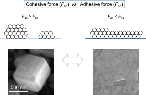
Copper iodide (CuI) is an emerging high-performance p-type, wide-band-gap semiconductor. However, the growth mechanisms of CuI thin films and nanocrystals are currently unclear, as they do not follow the established models. In this work, the growth mechanisms and kinetics of sputtered CuI thin films were studied, which mainly depended on adatom/substrate interface properties driven by growth temperature and rate. A modified structure zone model was proposed to explain the two-dimensional layer-by-layer and three-dimensional island growth of CuI with different rates. The Wulff shape of the isolated CuI nanocrystals appeared to be controllable by the available iodine ion flux at high temperatures but low growth rates near the equilibrium. Moreover, smooth CuI thin films were successfully produced by combining a high substrate temperature with a high growth rate. A record-high hole mobility in a high carrier-density range was demonstrated, which was greater than twice the values reported previously. Our findings represent the essential steps toward advanced materials engineering and fabrication of CuI thin films for practical devices, as well as the self-assembly of shape-controlled CuI nano- and microcrystals.
中文翻译:

用于高迁移率薄膜和自组装微晶的碘化铜的可控生长
碘化铜(CuI)是一种新兴的高性能p型宽带隙半导体。但是,CuI薄膜和纳米晶体的生长机理目前尚不清楚,因为它们没有遵循已建立的模型。在这项工作中,研究了溅射的CuI薄膜的生长机理和动力学,这主要取决于生长温度和速率驱动的原子/基底界面性质。提出了一种改进的结构区模型来解释CuI在不同速率下的二维逐层和三维岛状生长。分离的CuI纳米晶体的Wulff形状似乎可以通过在高温下可用的碘离子通量来控制,但是在平衡附近的生长速率较低。此外,通过将高衬底温度和高生长速率结合在一起,成功生产出光滑的CuI薄膜。结果表明,在高载流子密度范围内,空穴迁移率达到了创纪录的水平,比以前报道的值大两倍。我们的发现代表了先进材料工程和实用器件的CuI薄膜制造以及形状控制的CuI纳米和微晶自组装的关键步骤。
更新日期:2020-11-25
中文翻译:
用于高迁移率薄膜和自组装微晶的碘化铜的可控生长
碘化铜(CuI)是一种新兴的高性能p型宽带隙半导体。但是,CuI薄膜和纳米晶体的生长机理目前尚不清楚,因为它们没有遵循已建立的模型。在这项工作中,研究了溅射的CuI薄膜的生长机理和动力学,这主要取决于生长温度和速率驱动的原子/基底界面性质。提出了一种改进的结构区模型来解释CuI在不同速率下的二维逐层和三维岛状生长。分离的CuI纳米晶体的Wulff形状似乎可以通过在高温下可用的碘离子通量来控制,但是在平衡附近的生长速率较低。此外,通过将高衬底温度和高生长速率结合在一起,成功生产出光滑的CuI薄膜。结果表明,在高载流子密度范围内,空穴迁移率达到了创纪录的水平,比以前报道的值大两倍。我们的发现代表了先进材料工程和实用器件的CuI薄膜制造以及形状控制的CuI纳米和微晶自组装的关键步骤。


 京公网安备 11010802027423号