Nano Research ( IF 9.9 ) Pub Date : 2020-09-05 , DOI: 10.1007/s12274-020-3003-6 Changyong Lan , Xiaolin Kang , You Meng , Renjie Wei , Xiuming Bu , SenPo Yip , Johnny C. Ho
|
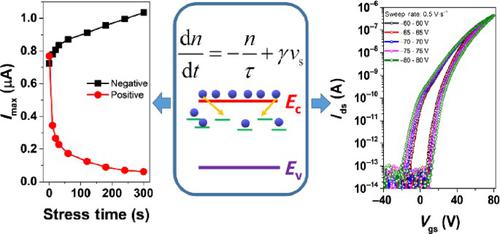
Due to the ultra-thin nature and moderate carrier mobility, semiconducting two-dimensional (2D) materials have attracted extensive attention for next-generation electronics. However, the gate bias stress instability and hysteresis are always observed in these 2D materials-based transistors that significantly degrade their reliability for practical applications. Herein, the origin of gate bias stress instability and hysteresis for chemical vapor deposited monolayer WS2 transistors are investigated carefully. The transistor performance is found to be strongly affected by the gate bias stress time, sweeping rate and range, and temperature. Based on the systematical study and complementary analysis, charge trapping is determined to be the major contribution for these observed phenomena. Importantly, due to these charge trapping effects, the channel current is observed to decrease with time; hence, a rate equation, considering the charge trapping and time decay effect of current, is proposed and developed to model the phenomena with excellent consistency with experimental data. All these results do not only indicate the validity of the charge trapping model, but also confirm the hysteresis being indeed caused by charge trapping. Evidently, this simple model provides a sufficient explanation for the charge trapping induced gate bias stress instability and hysteresis in monolayer WS2 transistors, which can be also applicable to other kinds of transistors.
中文翻译:
单层WS 2晶体管中栅极偏置应力的不稳定性和滞后性的起因
由于超薄特性和适中的载流子迁移率,半导体二维(2D)材料已引起下一代电子设备的广泛关注。但是,在这些基于2D材料的晶体管中始终观察到栅极偏置应力的不稳定性和磁滞现象,这严重降低了其在实际应用中的可靠性。这里,化学气相沉积单层WS 2的栅极偏置应力不稳定性和磁滞的起源仔细研究晶体管。发现晶体管的性能受栅极偏置应力时间,扫描速率和范围以及温度的强烈影响。根据系统研究和补充分析,电荷陷阱被确定为这些观察到的现象的主要贡献。重要的是,由于这些电荷俘获效应,观察到沟道电流随时间减少;因此,提出并考虑了电流的电荷俘获和时间衰减效应的速率方程,并建立了与实验数据具有良好一致性的模型。所有这些结果不仅表明电荷陷阱模型的有效性,而且证实了滞后确实是由电荷陷阱引起的。显然,2个晶体管,也可以应用于其他类型的晶体管。


 京公网安备 11010802027423号