当前位置:
X-MOL 学术
›
Prog. Photovoltaics
›
论文详情
Our official English website, www.x-mol.net, welcomes your feedback! (Note: you will need to create a separate account there.)
Analysis of the negative charges injected into a SiO2/SiNx stack using plasma charging technology for field‐effect passivation on a boron‐doped silicon surface
Progress in Photovoltaics ( IF 6.7 ) Pub Date : 2020-10-04 , DOI: 10.1002/pip.3340 Kwan Hong Min 1, 2 , Jeong‐Mo Hwang 3 , Eunwan Cho 4 , Hee‐eun Song 1 , Sungeun Park 1 , Ajeet Rohatgi 4 , Donghwan Kim 2, 5 , Hae‐Seok Lee 5 , Yoonmook Kang 5 , Young‐Woo Ok 4 , Min Gu Kang 1
Progress in Photovoltaics ( IF 6.7 ) Pub Date : 2020-10-04 , DOI: 10.1002/pip.3340 Kwan Hong Min 1, 2 , Jeong‐Mo Hwang 3 , Eunwan Cho 4 , Hee‐eun Song 1 , Sungeun Park 1 , Ajeet Rohatgi 4 , Donghwan Kim 2, 5 , Hae‐Seok Lee 5 , Yoonmook Kang 5 , Young‐Woo Ok 4 , Min Gu Kang 1
Affiliation
|
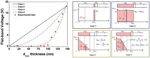
We investigated field‐effect passivation by injecting negative charges into SiO2/SiNx stack using a plasma charge injection technique. The Si/SiO2/SiNx samples exhibited a very high flat‐band shift with a high injected negative charge density (>3.0 × 1013 cm2) after plasma negative charge injection; this density was higher than that for the well‐known Al2O3 layer. Most injected negative charges were present within approximately 90 nm of the surface of the SiNx layer deposited by plasma‐enhanced chemical vapor deposition (PECVD) when comparing the capacitance–voltage analysis results obtained while etching the SiNx film considering four assumptions of the injected negative charge distribution. The saturation current density in a 90‐ohm/sq boron emitter decreased from ~90 to 50 fA/cm2 after negative charge injection, which is equivalent to the J0e of the structure passivated with an Al2O3/SiNx stack. Six‐inch n‐type bifacial cells with an approximately 100‐ohm/sq boron emitter passivated with SiO2/SiNx displayed an approximately 0.2% increase in absolute cell efficiency after negative charge injection. In addition, n‐PERT bifacial cells with a high boron sheet resistance of ~150 ohm/sq exhibited a 1.0% or higher absolute efficiency enhancement from a relatively low precharging efficiency of approximately 19.0%. We also demonstrated that the final efficiency after charging was comparable with n‐PERT bifacial cells with Al2O3 passivation, suggesting that the proposed process is a potential low‐cost alternative method that could replace expensive Al2O3 processes.
中文翻译:

使用等离子充电技术分析掺入SiO2 / SiNx堆叠中的负电荷以在掺硼硅表面上进行场效应钝化
通过使用等离子注入技术将负电荷注入SiO 2 / SiN x堆中,我们研究了场效应钝化。等离子体负电荷注入后,Si / SiO 2 / SiN x样品表现出非常高的平带位移和高注入负电荷密度(> 3.0×10 13 cm 2)。该密度高于众所周知的Al 2 O 3层。大多数注入的负电荷存在于SiN x表面约90 nm内当比较注入的负电荷分布的四个假设时,在蚀刻SiN x膜时获得的电容-电压分析结果进行比较时,通过等离子体增强化学气相沉积(PECVD)沉积的硅层。负电荷注入后,90Ω/ sq的硼发射极中的饱和电流密度从〜90降至50 fA / cm 2,这相当于用Al 2 O 3 / SiN x叠层钝化的结构的J 0e。具有SiO 2 / SiN x钝化的约100 ohm / sq硼发射极的六英寸n型双面电池在注入负电荷后,绝对电池效率提高了约0.2%。此外,具有约150 ohm / sq的高硼薄层电阻的n ‐PERT双面电池显示出1.0%或更高的绝对效率增强,而相对较低的预充电效率约为19.0%。我们还证明,充电后的最终效率与具有Al 2 O 3钝化的n ‐PERT双面电池相当,这表明所提出的工艺是一种潜在的低成本替代方法,可以替代昂贵的Al 2 O 3工艺。
更新日期:2020-10-04
中文翻译:
使用等离子充电技术分析掺入SiO2 / SiNx堆叠中的负电荷以在掺硼硅表面上进行场效应钝化
通过使用等离子注入技术将负电荷注入SiO 2 / SiN x堆中,我们研究了场效应钝化。等离子体负电荷注入后,Si / SiO 2 / SiN x样品表现出非常高的平带位移和高注入负电荷密度(> 3.0×10 13 cm 2)。该密度高于众所周知的Al 2 O 3层。大多数注入的负电荷存在于SiN x表面约90 nm内当比较注入的负电荷分布的四个假设时,在蚀刻SiN x膜时获得的电容-电压分析结果进行比较时,通过等离子体增强化学气相沉积(PECVD)沉积的硅层。负电荷注入后,90Ω/ sq的硼发射极中的饱和电流密度从〜90降至50 fA / cm 2,这相当于用Al 2 O 3 / SiN x叠层钝化的结构的J 0e。具有SiO 2 / SiN x钝化的约100 ohm / sq硼发射极的六英寸n型双面电池在注入负电荷后,绝对电池效率提高了约0.2%。此外,具有约150 ohm / sq的高硼薄层电阻的n ‐PERT双面电池显示出1.0%或更高的绝对效率增强,而相对较低的预充电效率约为19.0%。我们还证明,充电后的最终效率与具有Al 2 O 3钝化的n ‐PERT双面电池相当,这表明所提出的工艺是一种潜在的低成本替代方法,可以替代昂贵的Al 2 O 3工艺。


 京公网安备 11010802027423号