当前位置:
X-MOL 学术
›
Appl. Surf. Sci.
›
论文详情
Our official English website, www.x-mol.net, welcomes your feedback! (Note: you will need to create a separate account there.)
Extending the near-infrared band-edge absorption spectrum of silicon by proximity to a 2D semiconductor
Applied Surface Science ( IF 6.7 ) Pub Date : 2021-02-01 , DOI: 10.1016/j.apsusc.2020.147803 Valerio Apicella , Teslim Ayinde Fasasi , Hon Fai Wong , Dennis C.W. Leung , Antonio Ruotolo
Applied Surface Science ( IF 6.7 ) Pub Date : 2021-02-01 , DOI: 10.1016/j.apsusc.2020.147803 Valerio Apicella , Teslim Ayinde Fasasi , Hon Fai Wong , Dennis C.W. Leung , Antonio Ruotolo
|
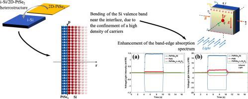
Because of its low-cost, silicon is the standard material for photovoltaic conversion. Yet, its band-edge absorption spectrum is narrower than the spectrum of the solar radiation, which reduces its conversion efficiency. In this paper, it is shown that the spectrum of absorbance of silicon can be extended to longer wavelengths by proximity to a two-dimensional (2D) semiconductor. Photo-induced Hall effect, together with standard absorption spectroscopy, was employed to estimate the increase of efficiency of absorbance of a 2D-platinum-diselenide/intrinsic-silicon bilayer. The bilayer shows a significantly higher absorption in the infrared as compared to the single films. Moreover, an overall increase of absorption efficiency by a factor twenty was measured in the entire spectrum of light of a halogen lamp. X-ray Photoelectron Spectroscopy (XPS) confirms that a reduction of the band-gap occurs in the silicon substrate at the interface between the two semiconductors. The results are interpreted in the framework of band-gap narrowing due to hole-plasma confinement in the Si, induced by electron-confinement in the 2D film. Possible application of the effect in photo-voltaic cells is discussed.
中文翻译:

通过接近二维半导体扩展硅的近红外带边吸收光谱
由于成本低,硅是光伏转换的标准材料。然而,它的带边吸收光谱比太阳辐射的光谱窄,这降低了它的转换效率。在本文中,表明通过接近二维 (2D) 半导体,硅的吸收光谱可以扩展到更长的波长。光致霍尔效应与标准吸收光谱一起被用来估计 2D-铂-二硒化物/本征-硅双层的吸收效率的增加。与单层膜相比,双层膜在红外线中显示出明显更高的吸收。此外,在卤素灯的整个光谱中测量到吸收效率整体增加了 20 倍。X 射线光电子能谱 (XPS) 证实,在两个半导体之间的界面处的硅衬底中发生带隙减小。结果是在带隙变窄的框架内解释的,这是由于 2D 薄膜中的电子限制引起的 Si 中的空穴等离子体限制。讨论了该效应在光伏电池中的可能应用。
更新日期:2021-02-01
中文翻译:
通过接近二维半导体扩展硅的近红外带边吸收光谱
由于成本低,硅是光伏转换的标准材料。然而,它的带边吸收光谱比太阳辐射的光谱窄,这降低了它的转换效率。在本文中,表明通过接近二维 (2D) 半导体,硅的吸收光谱可以扩展到更长的波长。光致霍尔效应与标准吸收光谱一起被用来估计 2D-铂-二硒化物/本征-硅双层的吸收效率的增加。与单层膜相比,双层膜在红外线中显示出明显更高的吸收。此外,在卤素灯的整个光谱中测量到吸收效率整体增加了 20 倍。X 射线光电子能谱 (XPS) 证实,在两个半导体之间的界面处的硅衬底中发生带隙减小。结果是在带隙变窄的框架内解释的,这是由于 2D 薄膜中的电子限制引起的 Si 中的空穴等离子体限制。讨论了该效应在光伏电池中的可能应用。


 京公网安备 11010802027423号