当前位置:
X-MOL 学术
›
Int. J. Circ. Theory Appl.
›
论文详情
Our official English website, www.x-mol.net, welcomes your feedback! (Note: you will need to create a separate account there.)
New simple transistor realizations of second‐ generation voltage conveyor
International Journal of Circuit Theory and Applications ( IF 2.3 ) Pub Date : 2020-09-27 , DOI: 10.1002/cta.2879 Abdullah Yesil 1 , Shahram Minaei 2
International Journal of Circuit Theory and Applications ( IF 2.3 ) Pub Date : 2020-09-27 , DOI: 10.1002/cta.2879 Abdullah Yesil 1 , Shahram Minaei 2
Affiliation
|
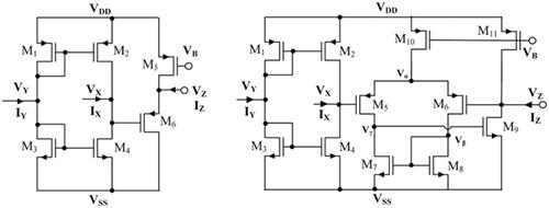
In this paper, two new complementary metal oxide semiconductor (CMOS) realizations for second‐generation voltage conveyor (VCII) are presented. The first proposed VCII has a very simple structure employing only six transistors. The second proposed VCII employs 11 transistors, and none of the transistors at both proposed circuits suffer from the body effect. Small‐signal analysis, parasitic elements, and input‐referred noise of the proposed VCIIs are given. Moreover, a new active element called voltage controlled second‐generation voltage conveyor (VC‐VCII) is proposed as dual element of current controlled second‐generation current conveyor (CCCII) active element. Its parasitic resistance at the Y terminal can be controlled electronically. Two presented CMOS structures of VCII are worked as VC‐VCII with slight modification. Proposed circuits are simulated in Cadence Analog environment using TSMC 0.18‐μm process parameters with ±0.9‐V supply voltages. Both CMOS structures occupy a small chip area of 276.8 and 271 μm2, respectively. The bandwidth of the current follower stage of the proposed VCIIs is found as 794 MHz, whereas the bandwidth of the voltage follower stage for the first and second proposed VCIIs is found as 2.57 and 1.92 GHz, respectively. As an application example, voltage‐mode first‐order low‐pass filter has been given with its tunable gain by using VC‐VCII.
中文翻译:

第二代电压传送器的新的简单晶体管实现
本文介绍了用于第二代电压传送器(VCII)的两个新的互补金属氧化物半导体(CMOS)实现。首先提出的VCII具有仅使用六个晶体管的非常简单的结构。提出的第二个VCII使用11个晶体管,并且两个提议的电路中的所有晶体管都没有受到人体效应的影响。给出了拟议VCII的小信号分析,寄生元件和输入参考噪声。此外,提出了一种称为电压控制第二代电压传送器(VC-VCII)的新型有源元件,作为电流控制第二代电流传送器(CCCII)有源元件的双重元件。在Y方向的寄生电阻终端可以电子控制。VCII的两种提出的CMOS结构都可以作为VC‐VCII进行稍加修改。在Cadence Analog环境中使用TSMC0.18-μm工艺参数和±0.9-V电源电压对拟议电路进行仿真。两个CMOS结构占据的276.8和271微米小的芯片面积2,分别。提出的VCII的电流跟随器级的带宽为794 MHz,而提出的第一和第二个VCII的电压跟随器级的带宽分别为2.57和1.92 GHz。作为一个应用示例,电压模式一阶低通滤波器已通过使用VC-VCII进行了可调增益。
更新日期:2020-11-06
中文翻译:
第二代电压传送器的新的简单晶体管实现
本文介绍了用于第二代电压传送器(VCII)的两个新的互补金属氧化物半导体(CMOS)实现。首先提出的VCII具有仅使用六个晶体管的非常简单的结构。提出的第二个VCII使用11个晶体管,并且两个提议的电路中的所有晶体管都没有受到人体效应的影响。给出了拟议VCII的小信号分析,寄生元件和输入参考噪声。此外,提出了一种称为电压控制第二代电压传送器(VC-VCII)的新型有源元件,作为电流控制第二代电流传送器(CCCII)有源元件的双重元件。在Y方向的寄生电阻终端可以电子控制。VCII的两种提出的CMOS结构都可以作为VC‐VCII进行稍加修改。在Cadence Analog环境中使用TSMC0.18-μm工艺参数和±0.9-V电源电压对拟议电路进行仿真。两个CMOS结构占据的276.8和271微米小的芯片面积2,分别。提出的VCII的电流跟随器级的带宽为794 MHz,而提出的第一和第二个VCII的电压跟随器级的带宽分别为2.57和1.92 GHz。作为一个应用示例,电压模式一阶低通滤波器已通过使用VC-VCII进行了可调增益。


 京公网安备 11010802027423号