当前位置:
X-MOL 学术
›
ACS Appl. Electron. Mater.
›
论文详情
Our official English website, www.x-mol.net, welcomes your feedback! (Note: you will need to create a separate account there.)
Nanocrystalline and Polycrystalline β-Ga2O3 Thin Films for Deep Ultraviolet Detectors
ACS Applied Electronic Materials ( IF 4.7 ) Pub Date : 2020-09-21 , DOI: 10.1021/acsaelm.0c00643 Maria Isabel Pintor-Monroy 1 , Bayron L. Murillo-Borjas 1 , Manuel A. Quevedo-Lopez 1
ACS Applied Electronic Materials ( IF 4.7 ) Pub Date : 2020-09-21 , DOI: 10.1021/acsaelm.0c00643 Maria Isabel Pintor-Monroy 1 , Bayron L. Murillo-Borjas 1 , Manuel A. Quevedo-Lopez 1
Affiliation
|
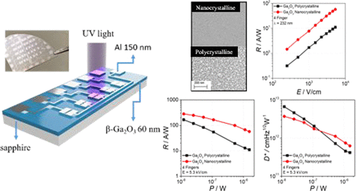
The wide band gap and high breakdown field of β-Ga2O3 single crystals and thin films have recently attracted considerable attention not only for high-power applications, fabricating devices such as transistors and diodes, but also for several other applications such as deep-UV (DUV) sensors, with a cutoff at ∼280 nm, resulting in visible-blind detectors. Currently, most of the UV- and DUV-based simple metal–semiconductor–metal (MSM) systems use interdigitated electrodes, which requires high-quality, defect-free films. β-Ga2O3 films deposited by simple methods such as magnetron sputtering are scarce, and most high-quality β-Ga2O3 thin films have been demonstrated using pulsed laser deposition (PLD) and molecular beam epitaxy (MBE). Herein, we show a comprehensive study to effectively control the structural, optical, and electrical properties of β-Ga2O3 thin films deposited by sputtering. Highly oriented polycrystalline or nanocrystalline n-type β-Ga2O3 thin films were deposited by this method and evaluated as DUV detectors using a simple MSM structure under DUV light with 254 and 232 nm wavelengths. Different structures—varying the number of fingers—are evaluated, under different light intensities and applying different electric fields. High responsivities are obtained, especially for nanocrystalline β-Ga2O3 thin films. The high responsivity for both films is attributed to self-trapped holes resulting in an internal gain. Higher responsivity is also observed for higher electric fields, lower light intensities, and a smaller number of fingers. Rise and decay times are comparable, in the range of 11–13 and 14–15 ms, respectively. Our results indicate that sputtered β-Ga2O3 thin films are promising for visible-blind DUV detectors. The paper also demonstrates simple strategies to control the crystallinity of sputtered β-Ga2O3 thin films.
中文翻译:

纳米晶和多晶的β-Ga 2 ö 3薄膜深紫外探测器
宽带隙和高击穿场的β-Ga 2 ö 3单晶和薄膜最近引起相当大的关注,不仅用于高功率应用中,制造设备,诸如晶体管和二极管,但也可用于其它一些应用,例如深-UV(DUV)传感器,截止波长约为280 nm,因此产生了可见盲检测器。当前,大多数基于UV和DUV的简单金属-半导体-金属(MSM)系统都使用叉指电极,这需要高质量,无缺陷的薄膜。的β-Ga 2层ö 3通过简单的方法沉积膜,如磁控溅射稀少,和最优质的β-Ga 2 ö 3已经使用脉冲激光沉积(PLD)和分子束外延(MBE)证明了薄膜。此,我们表明了全面的研究,以有效地控制的β-Ga的结构,光学和电学性质2 ö 3通过溅射沉积的薄膜。高度取向的多晶或纳米晶体的n型的β-Ga 2个ö 3薄膜通过该方法沉积并评价为使用下DUV光的简单MSM结构254米232纳米的波长的DUV探测器。在不同的光强度和施加不同的电场的情况下,将评估不同的结构(即手指的数量)。获得高响应度,尤其是对于纳米晶体的β-Ga 2 ö 3薄膜。两种膜的高响应性都归因于自陷孔,导致内部增益。对于较高的电场,较低的光强度和较少的手指,也观察到较高的响应度。上升时间和下降时间相当,分别在11-13和14-15 ms的范围内。我们的研究结果表明,溅射的β-Ga 2 ö 3层薄膜是有希望的可见-不可见DUV探测器。本文还说明了简单的策略来控制溅射的β-Ga的结晶2 ö 3薄膜。
更新日期:2020-10-28
中文翻译:
纳米晶和多晶的β-Ga 2 ö 3薄膜深紫外探测器
宽带隙和高击穿场的β-Ga 2 ö 3单晶和薄膜最近引起相当大的关注,不仅用于高功率应用中,制造设备,诸如晶体管和二极管,但也可用于其它一些应用,例如深-UV(DUV)传感器,截止波长约为280 nm,因此产生了可见盲检测器。当前,大多数基于UV和DUV的简单金属-半导体-金属(MSM)系统都使用叉指电极,这需要高质量,无缺陷的薄膜。的β-Ga 2层ö 3通过简单的方法沉积膜,如磁控溅射稀少,和最优质的β-Ga 2 ö 3已经使用脉冲激光沉积(PLD)和分子束外延(MBE)证明了薄膜。此,我们表明了全面的研究,以有效地控制的β-Ga的结构,光学和电学性质2 ö 3通过溅射沉积的薄膜。高度取向的多晶或纳米晶体的n型的β-Ga 2个ö 3薄膜通过该方法沉积并评价为使用下DUV光的简单MSM结构254米232纳米的波长的DUV探测器。在不同的光强度和施加不同的电场的情况下,将评估不同的结构(即手指的数量)。获得高响应度,尤其是对于纳米晶体的β-Ga 2 ö 3薄膜。两种膜的高响应性都归因于自陷孔,导致内部增益。对于较高的电场,较低的光强度和较少的手指,也观察到较高的响应度。上升时间和下降时间相当,分别在11-13和14-15 ms的范围内。我们的研究结果表明,溅射的β-Ga 2 ö 3层薄膜是有希望的可见-不可见DUV探测器。本文还说明了简单的策略来控制溅射的β-Ga的结晶2 ö 3薄膜。


 京公网安备 11010802027423号