Nano Energy ( IF 17.6 ) Pub Date : 2020-09-17 , DOI: 10.1016/j.nanoen.2020.105390 Xiaoyang Chen , Biaolin Peng , MingJian Ding , Xiaoshan Zhang , Bin Xie , Taolan Mo , Qi Zhang , Ping Yu , Zhong Lin Wang
|
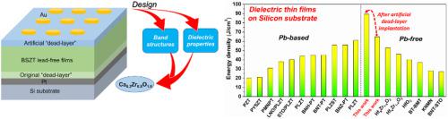
High-performance lead-free thin-film capacitors deposited on the silicon (Si) wafers with large energy storage density (W) and high reliability are strongly attractive in the modern electrical and electronic devices. Here, an ultrahigh W was achieved in the Ba0.3Sr0.7Zr0.18Ti0.82O3 (BSZT) relaxor ferroelectric thin films deposited on the Si wafers with the help of an ultrathin Ca0.2Zr0.8O1.8 (CSZ) artificial “dead-layer” simultaneously possessing high resistivity, wide band gap and high permittivity among linear dielectrics. As the CSZ was implanted, the W of the Ba0.3Sr0.7Zr0.18Ti0.82O3 (BSZT) thin films was greatly increased from 64.9 J/cm3 to 89.4 J/cm3, which is comparable to the best W of thin film deposited on expensive single crystal substrates, and is the largest one reported so far than those of lead-free thin films deposited on the Si wafers, and even for lead thin films. Due to the formation of ultrahigh electrons injection barrier (3.92 eV) between the interface of the CSZ dead layer and the Au top electrode, the Schottky emission of the BSZT thin films under high electric field and at high temperatures was effective suppressed, which is responsible for the greatly improved dielectric breakdown strength and thermal stability. Moreover, the fatigue endurance was also enhanced. It is concluded that the implantation of the CSZ artificial dead-layer could be used as a universal-simple-effective strategy to improve the electrical performances of ferroelectric materials working in the harsh environment of high electric field.
中文翻译:
具有人工死层的Si晶片上沉积的无铅介电薄膜中的巨大储能密度
具有高储能密度(W)和高可靠性的,沉积在硅(Si)晶片上的高性能无铅薄膜电容器在现代电气和电子设备中非常有吸引力。在这里,借助于超薄Ca 0.2 Zr 0.8 O 1.8(CSZ)人工“死角”,在Si晶片上沉积的Ba 0.3 Sr 0.7 Zr 0.18 Ti 0.82 O 3(BSZT)弛豫铁电薄膜中实现了超高W。线性电介质之间同时具有高电阻率,宽带隙和高介电常数。植入CSZ时,WBa 0.3 Sr 0.7 Zr 0.18 Ti 0.82 O 3(BSZT)薄膜的膜厚从64.9 J / cm 3增加到89.4 J / cm 3,与最佳W相当。沉积在昂贵的单晶衬底上的薄膜的数量最多,是迄今为止报道的最大数量的薄膜,其沉积量超过了沉积在Si晶片上的无铅薄膜,甚至铅薄膜。由于在CSZ死层和Au顶部电极的界面之间形成了超高电子注入势垒(3.92 eV),有效抑制了BSZT薄膜在高电场和高温下的肖特基发射,这是有原因的大大提高了介电击穿强度和热稳定性。此外,疲劳强度也得到了提高。结论是,CSZ人工死层的植入可以作为一种通用的,有效的策略,以改善在强电场条件下工作的铁电材料的电性能。


 京公网安备 11010802027423号