Sensors and Actuators A: Physical ( IF 4.6 ) Pub Date : 2020-09-15 , DOI: 10.1016/j.sna.2020.112333 V. Balasubramani , J. Chandrasekaran , Tien Dai Nguyen , S. Maruthamuthu , R. Marnadu , P. Vivek , S. Sugarthi
|
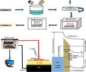
In the present work, we have fabricated a highly photo responsive Schottky barrier diode based on cerium infused vanadium pentoxide thin film (Ce-V2O5) as a interfacial layer. It was coated on a glass slide by low-cost sol-gel spin-coating technique and annealed at 500 °C. Structure, surface morphology, optical and electrical characteristic of Ce infused V2O5 films with different Ce concentrations viz 0, 2, 4 and 6 wt% were investigated. X-ray diffraction (XRD) pattern exposed that all coated films are tetragonal structure. And a peak shift was recorded after doping Ce ion into the V2O5 system. FE-SEM images showed a smooth nanorods and nanoplate-like structures in nano-scale region. Topology view by AFM showed a significant decrease in surface roughness of the film at different wt.% of Ce. The incorporation of Ce concentration based on the optical absorbance and band gap energy were studied, using UV–vis spectroscopy. Current-voltage (I–V), characteristics, photo-diode parameters of the Cu/Ce-V2O5/n-Si diodes were evaluated under dark and light exposed conditions. A maximum quantum efficiency of 25.54 % was achieved for the MIS diode fabricated with 6 % of Ce. The photosensitivity of the Cu/Ce-V2O5/n-Si diode 100 times higher than pure diode. Photodiode parameters and I–V analysis revealed that Ce with 6 wt.% is appropriate for the development of high quality photodiode and photo detector applications based to its electrical-performance.
中文翻译:
MIS结构的Ce-V 2 O 5界面层对肖特基二极管行为的巨大光敏增强作用
在目前的工作中,我们已经制备了一种高光响应肖特基势垒二极管,该器件基于注入铈的五氧化二钒薄膜(Ce-V 2 O 5)作为界面层。通过低成本的溶胶-凝胶旋涂技术将其涂布在载玻片上,并在500°C下退火。研究了不同浓度Ce分别为0、2、4和6 wt%的Ce注入V 2 O 5薄膜的结构,表面形态,光学和电学特性。X射线衍射(XRD)图样显示,所有涂膜均为四方结构。将Ce离子掺杂到V 2 O 5中后,记录到峰位移系统。FE-SEM图像显示出纳米级区域内的光滑纳米棒和纳米板状结构。通过AFM的拓扑图显示,在不同的Ce重量%下,膜的表面粗糙度显着降低。使用紫外可见光谱研究了基于吸光度和带隙能量的铈浓度的掺入。Cu / Ce-V 2 O 5 / n-Si二极管的电流-电压(IV),特性,光电二极管参数在黑暗和光照条件下进行了评估。用6%Ce制成的MIS二极管的最大量子效率达到25.54%。Cu / Ce-V 2 O 5的光敏性/ n-Si二极管比纯二极管高100倍。光电二极管参数和I–V分析表明,具有6 wt。%的Ce的电气性能适合于开发高质量光电二极管和光电检测器应用。


 京公网安备 11010802027423号