Our official English website, www.x-mol.net, welcomes your feedback! (Note: you will need to create a separate account there.)
Quantum Transport in Two-Dimensional WS2 with High-Efficiency Carrier Injection through Indium Alloy Contacts.
ACS Nano ( IF 17.1 ) Pub Date : 2020-09-11 , DOI: 10.1021/acsnano.0c05915 Chit Siong Lau 1 , Jing Yee Chee 1 , Yee Sin Ang 2 , Shi Wun Tong 1 , Liemao Cao 2, 3 , Zi-En Ooi 1 , Tong Wang 1 , Lay Kee Ang 2 , Yan Wang 4 , Manish Chhowalla 4 , Kuan Eng Johnson Goh 1, 5
ACS Nano ( IF 17.1 ) Pub Date : 2020-09-11 , DOI: 10.1021/acsnano.0c05915 Chit Siong Lau 1 , Jing Yee Chee 1 , Yee Sin Ang 2 , Shi Wun Tong 1 , Liemao Cao 2, 3 , Zi-En Ooi 1 , Tong Wang 1 , Lay Kee Ang 2 , Yan Wang 4 , Manish Chhowalla 4 , Kuan Eng Johnson Goh 1, 5
Affiliation
|
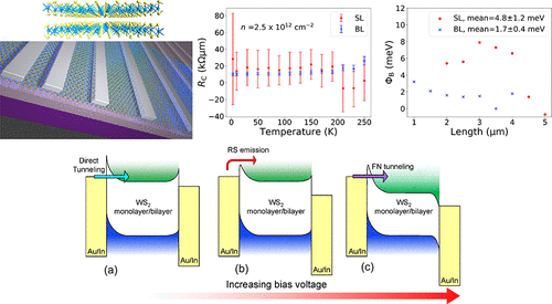
Two-dimensional transition metal dichalcogenides (TMDCs) have properties attractive for optoelectronic and quantum applications. A crucial element for devices is the metal–semiconductor interface. However, high contact resistances have hindered progress. Quantum transport studies are scant as low-quality contacts are intractable at cryogenic temperatures. Here, temperature-dependent transfer length measurements are performed on chemical vapor deposition grown single-layer and bilayer WS2 devices with indium alloy contacts. The devices exhibit low contact resistances and Schottky barrier heights (∼10 kΩ μm at 3 K and 1.7 meV). Efficient carrier injection enables high carrier mobilities (∼190 cm2 V–1 s–1) and observation of resonant tunnelling. Density functional theory calculations provide insights into quantum transport and properties of the WS2–indium interface. Our results reveal significant advances toward high-performance WS2 devices using indium alloy contacts.
中文翻译:

通过高效率载流子注入通过铟合金触点实现的二维WS2中的量子传输。
二维过渡金属二硫化碳(TMDC)具有吸引光电和量子应用的特性。设备的关键要素是金属-半导体界面。然而,高接触电阻阻碍了进展。量子传输研究很少,因为在低温下难以获得低质量的接触。在此,对与铟合金接触的化学气相沉积生长的单层和双层WS 2器件执行与温度相关的传输长度测量。该器件具有较低的接触电阻和肖特基势垒高度(在3 K和1.7 meV时约为10kΩμm)。高效的载流子注入可实现高载流子迁移率(〜190 cm 2 V –1 s –1)并观察共振隧穿。密度泛函理论计算提供了有关WS 2-铟界面的量子输运和性质的见解。我们的结果表明,使用铟合金触点的高性能WS 2器件取得了显着进步。
更新日期:2020-10-28
中文翻译:
通过高效率载流子注入通过铟合金触点实现的二维WS2中的量子传输。
二维过渡金属二硫化碳(TMDC)具有吸引光电和量子应用的特性。设备的关键要素是金属-半导体界面。然而,高接触电阻阻碍了进展。量子传输研究很少,因为在低温下难以获得低质量的接触。在此,对与铟合金接触的化学气相沉积生长的单层和双层WS 2器件执行与温度相关的传输长度测量。该器件具有较低的接触电阻和肖特基势垒高度(在3 K和1.7 meV时约为10kΩμm)。高效的载流子注入可实现高载流子迁移率(〜190 cm 2 V –1 s –1)并观察共振隧穿。密度泛函理论计算提供了有关WS 2-铟界面的量子输运和性质的见解。我们的结果表明,使用铟合金触点的高性能WS 2器件取得了显着进步。


 京公网安备 11010802027423号