当前位置:
X-MOL 学术
›
Adv. Electron. Mater.
›
论文详情
Our official English website, www.x-mol.net, welcomes your feedback! (Note: you will need to create a separate account there.)
Coating Thickness Controls Crystallinity and Enables Homoepitaxial Growth of Ultra‐Thin‐Channel Blade‐Coated In2O3 Transistors
Advanced Electronic Materials ( IF 6.2 ) Pub Date : 2020-09-11 , DOI: 10.1002/aelm.202000354 Ahmad R. Kirmani 1 , Huilang Chen 1 , Christopher M. Stafford 1 , Emily G. Bittle 2 , Lee J. Richter 1
Advanced Electronic Materials ( IF 6.2 ) Pub Date : 2020-09-11 , DOI: 10.1002/aelm.202000354 Ahmad R. Kirmani 1 , Huilang Chen 1 , Christopher M. Stafford 1 , Emily G. Bittle 2 , Lee J. Richter 1
Affiliation
|
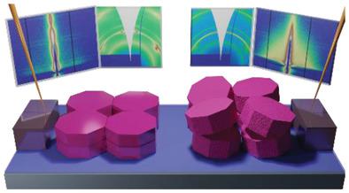
Scalable, solution‐deposited metal oxide (MO) thin films could enable low‐cost, flexible, large‐area electronics; however, the poor morphology of the typically polycrystalline films limits performance. It is demonstrated that optimized coating thickness leads to high‐quality crystalline films in blade‐coated indium oxide (In2O3) ultra‐thin‐film (8 nm) transistors (TFTs). TFTs are fabricated with total channel thickness ranging from 2 to 16 nm via varied multistep processes. Transport in channels fabricated from sequential, thin (≤4 nm) coatings significantly exceeds that from thicker coatings. A marked change is found in the In2O3 crystal texture with coating thickness. Single, thin coatings ≤4 nm produce smooth films with strong (111) texture while thicker coatings are rougher and exhibit little texture. Sequential thin coatings exhibit homoepitaxy. In addition to the improved transport due to the smooth, aligned films, it is found that deposition of sequential thin layers leads to the highest mobility, with either In2O3 or ZnO as the overcoat. This suggests defects at the air interface of the initial thin films limit performance. Optimizing coating thickness and sequence, it is demonstrated 8 nm thick channel In2O3 TFTs exhibiting percolation conduction with an impressive average saturation electron mobility (μsat) of (36.1 ± 0.9) cm2 V−1 s−1 (best‐performing device of 58.0 cm2 V−1 s−1).
中文翻译:

涂层厚度可控制结晶度并实现超薄通道刀片涂层In2O3晶体管的同质外延生长
可扩展的溶液沉积金属氧化物(MO)薄膜可以实现低成本,灵活的大面积电子产品。然而,典型的多晶膜的不良形态限制了性能。事实证明,优化的涂层厚度可在刀片涂层的氧化铟(In 2 O 3)超薄膜(8 nm)晶体管(TFT)中产生高质量的晶体膜。通过不同的多步工艺,TFT的总沟道厚度为2至16 nm。由顺序的薄涂层(≤4nm)制成的通道中的传输量大大超过了较厚的涂层。在In 2 O 3中发现了明显的变化具有涂层厚度的晶体质地。≤4nm的单层薄涂层可产生具有强(111)纹理的光滑膜,而较厚的涂层则较粗糙且几乎没有纹理。顺序的薄涂层表现出同质性。除了由于光滑,对齐的薄膜而改善的传输性能外,还发现连续沉积的薄层可产生最高的迁移率,而In 2 O 3或ZnO作为外涂层。这表明初始薄膜的空气界面处的缺陷限制了性能。优化了涂层的厚度和顺序,证明了8 nm厚的In 2 O 3 TFT中的沟道表现出渗流传导,具有惊人的平均饱和电子迁移率(μsat)(36.1±0.9)cm 2 V -1 s -1(最佳性能器件为58.0 cm 2 V -1 s -1)。
更新日期:2020-11-19
中文翻译:
涂层厚度可控制结晶度并实现超薄通道刀片涂层In2O3晶体管的同质外延生长
可扩展的溶液沉积金属氧化物(MO)薄膜可以实现低成本,灵活的大面积电子产品。然而,典型的多晶膜的不良形态限制了性能。事实证明,优化的涂层厚度可在刀片涂层的氧化铟(In 2 O 3)超薄膜(8 nm)晶体管(TFT)中产生高质量的晶体膜。通过不同的多步工艺,TFT的总沟道厚度为2至16 nm。由顺序的薄涂层(≤4nm)制成的通道中的传输量大大超过了较厚的涂层。在In 2 O 3中发现了明显的变化具有涂层厚度的晶体质地。≤4nm的单层薄涂层可产生具有强(111)纹理的光滑膜,而较厚的涂层则较粗糙且几乎没有纹理。顺序的薄涂层表现出同质性。除了由于光滑,对齐的薄膜而改善的传输性能外,还发现连续沉积的薄层可产生最高的迁移率,而In 2 O 3或ZnO作为外涂层。这表明初始薄膜的空气界面处的缺陷限制了性能。优化了涂层的厚度和顺序,证明了8 nm厚的In 2 O 3 TFT中的沟道表现出渗流传导,具有惊人的平均饱和电子迁移率(μsat)(36.1±0.9)cm 2 V -1 s -1(最佳性能器件为58.0 cm 2 V -1 s -1)。


 京公网安备 11010802027423号