当前位置:
X-MOL 学术
›
J. Alloys Compd.
›
论文详情
Our official English website, www.x-mol.net, welcomes your feedback! (Note: you will need to create a separate account there.)
Mixed-phase β-Ga2O3 and SnO2 metal-semiconductor-metal photodetectors with extended detection range from 293 nm to 330 nm
Journal of Alloys and Compounds ( IF 6.2 ) Pub Date : 2021-02-01 , DOI: 10.1016/j.jallcom.2020.157080 Ming-Ming Fan , Ling Cao , Kang-Li Xu , Xiu-Yan Li
Journal of Alloys and Compounds ( IF 6.2 ) Pub Date : 2021-02-01 , DOI: 10.1016/j.jallcom.2020.157080 Ming-Ming Fan , Ling Cao , Kang-Li Xu , Xiu-Yan Li
|
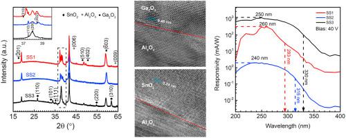
Abstract In this article, we demonstrate β-Ga2O3 and SnO2 mixed-phase thin films with dominant ( 2 ¯ 01)-β-Ga2O3 and (200)-SnO2 orientations on c-face sapphire (c-Al2O3) by chemical vapor deposition in a tube furnace. Transmission electron microscopy (TEM) reveals their simultaneous growth on substrate due to the small mismatches of ( 2 ¯ 01)-β-Ga2O3/c-Al2O3 (∼3%) and (200)-SnO2/c-Al2O3 (∼0.6%). Therefore, we also successfully demonstrate preferred-orientation ( 2 ¯ 01)-β-Ga2O3 and (200)-SnO2 mixed-phase thin films by controlling the Sn and Ga ratios in precursors. At 40 V, the photoelectric properties of metal-semiconductor-metal (MSM) photodetectors are modulated with more SnO2 content in mixed-phase thin films, including the dark current from 11 pA to 4 nA, the peak response in UVC from 240 nm (2 mA/W) to 260 nm (1.15 A/W), the tunable cut-off wavelength from 274 nm to 297 nm, and the extended detection range at long wavelength from 293 nm to 330 nm. Our devices show Ga2O3-like photoresponse properties rather than SnO2-like properties with lower dark current, comparable responsivity and detectivity, and faster response time than the performances of parts of the pure and mixed-phase Ga2O3-based photodetectors with untunable detection rang, which is expected to extend wider applications of other Ga2O3-based mixed-phase materials during doping or alloying, and paves a new and feasible way to realize high-performance Ga2O3-based photodetectors with controllable detection range.
中文翻译:

混合相 β-Ga2O3 和 SnO2 金属-半导体-金属光电探测器,探测范围从 293 nm 扩展到 330 nm
摘要 在本文中,我们通过化学气相沉积在 c 面蓝宝石 (c-Al2O3) 上展示了具有主要 (2¯ 01)-β-Ga2O3 和 (200)-SnO2 取向的 β-Ga2O3 和 SnO2 混合相薄膜。管式炉。由于 (2¯ 01)-β-Ga2O3/c-Al2O3 (~3%) 和 (200)-SnO2/c-Al2O3 (~0.6%) 的小失配,透射电子显微镜 (TEM) 显示它们在基板上同时生长)。因此,我们还通过控制前驱体中的 Sn 和 Ga 比例,成功地证明了优选取向的 (2¯01)-β-Ga2O3 和 (200)-SnO2 混合相薄膜。在 40 V 时,金属-半导体-金属 (MSM) 光电探测器的光电特性受到混合相薄膜中更多 SnO2 含量的调节,包括从 11 pA 到 4 nA 的暗电流,从 240 nm 的 UVC 峰值响应( 2 mA/W) 至 260 nm (1.15 A/W),274 nm 至 297 nm 的可调截止波长,以及 293 nm 至 330 nm 的长波长检测范围扩展。我们的器件显示出类似 Ga2O3 的光响应特性,而不是类似 SnO2 的特性,与具有不可调检测范围的纯和混合相 Ga2O3 基光电探测器的部分性能相比,具有更低的暗电流、可比的响应度和探测率以及更快的响应时间,其中有望在掺杂或合金化过程中扩展其他 Ga2O3 基混合相材料的更广泛应用,并为实现具有可控检测范围的高性能 Ga2O3 基光电探测器铺平了新的可行途径。
更新日期:2021-02-01
中文翻译:
混合相 β-Ga2O3 和 SnO2 金属-半导体-金属光电探测器,探测范围从 293 nm 扩展到 330 nm
摘要 在本文中,我们通过化学气相沉积在 c 面蓝宝石 (c-Al2O3) 上展示了具有主要 (2¯ 01)-β-Ga2O3 和 (200)-SnO2 取向的 β-Ga2O3 和 SnO2 混合相薄膜。管式炉。由于 (2¯ 01)-β-Ga2O3/c-Al2O3 (~3%) 和 (200)-SnO2/c-Al2O3 (~0.6%) 的小失配,透射电子显微镜 (TEM) 显示它们在基板上同时生长)。因此,我们还通过控制前驱体中的 Sn 和 Ga 比例,成功地证明了优选取向的 (2¯01)-β-Ga2O3 和 (200)-SnO2 混合相薄膜。在 40 V 时,金属-半导体-金属 (MSM) 光电探测器的光电特性受到混合相薄膜中更多 SnO2 含量的调节,包括从 11 pA 到 4 nA 的暗电流,从 240 nm 的 UVC 峰值响应( 2 mA/W) 至 260 nm (1.15 A/W),274 nm 至 297 nm 的可调截止波长,以及 293 nm 至 330 nm 的长波长检测范围扩展。我们的器件显示出类似 Ga2O3 的光响应特性,而不是类似 SnO2 的特性,与具有不可调检测范围的纯和混合相 Ga2O3 基光电探测器的部分性能相比,具有更低的暗电流、可比的响应度和探测率以及更快的响应时间,其中有望在掺杂或合金化过程中扩展其他 Ga2O3 基混合相材料的更广泛应用,并为实现具有可控检测范围的高性能 Ga2O3 基光电探测器铺平了新的可行途径。


 京公网安备 11010802027423号