当前位置:
X-MOL 学术
›
Cryst. Growth Des.
›
论文详情
Our official English website, www.x-mol.net, welcomes your feedback! (Note: you will need to create a separate account there.)
Comprehensive Analysis of Band Gap and Nanotwinning in Cd1–xMgxS QDs
Crystal Growth & Design ( IF 3.8 ) Pub Date : 2020-09-08 , DOI: 10.1021/acs.cgd.0c00851 Tania Kalsi 1 , Hrishit Mitra 2 , Tapta Kanchan Roy 2 , Sachin Kumar Godara 3 , Pragati Kumar 1
Crystal Growth & Design ( IF 3.8 ) Pub Date : 2020-09-08 , DOI: 10.1021/acs.cgd.0c00851 Tania Kalsi 1 , Hrishit Mitra 2 , Tapta Kanchan Roy 2 , Sachin Kumar Godara 3 , Pragati Kumar 1
Affiliation
|
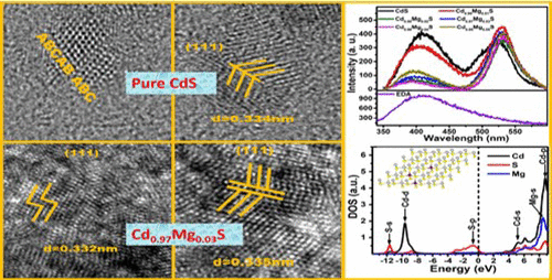
Planar defects, viz. stacking faults, grain boundaries, and twin boundaries, are observed in chemically synthesized Cd1–xMgxS quantum dots (QDs), with x ranging from 0 to 0.05 with an interval of 0.01. The density of nanotwins is augmented at the cost of stacking faults in Cd1–xMgxS QDs for x = 0.03, as revealed from high-resolution transmission electron microscopy (HRTEM). The interchange in defect density reflects an alteration in emission spectra. Astonishingly, we have observed above-band-gap emission (ABE) centered at ∼430 nm along with the usual below-band-gap emission centered at ∼526 nm. Emission above the band gap is perhaps exemplified for the first time for II–VI compound semiconductors and explicitly in Cd1–xMgxS QDs. The incorporation of Mg results in the band-gap tunability of CdS QDs as a consequence of synergetic effects of size variation and generation of new electronic states. For insight into the electronic states, density functional theory (DFT) based calculations were carried out. DFT calculations revealed that the substitution of Cd ions by Mg ions in the CdS creates electronic states of Mg just below the electronic state of Cd. Therefore, we assume that the modification in the band gap mainly results as a consequence of quantum confinement. The theoretical results qualitatively agree with the experimental outcomes of the present study.
中文翻译:

Cd 1– x Mg x S QD中带隙和纳米孪生的综合分析
平面缺陷,即。在化学合成的Cd 1– x Mg x S量子点(QDs)中观察到堆垛层错,晶界和孪晶界,x的范围从0到0.05,间隔为0.01。nanotwins的密度在镉的堆垛层错的成本被增大1- X的Mg X小号量子点为X= 0.03,如高分辨率透射电子显微镜(HRTEM)所揭示。缺陷密度的互换反映了发射光谱的变化。令人惊讶的是,我们观察到了以〜430 nm为中心的带隙以上发射(ABE),以及以〜526 nm为中心的通常的带隙下发射。对于II–VI化合物半导体,可能首次例举了带隙以上的发射,并且明确地以Cd 1– x Mg x的形式进行了举例说明。S QD。Mg的掺入导致CdS QD的带隙可调性,这是尺寸变化和产生新电子态的协同效应的结果。为了深入了解电子状态,进行了基于密度泛函理论(DFT)的计算。DFT计算表明,在CdS中用Mg离子取代Cd离子会产生Mg的电子态,其电子态刚好低于Cd的电子态。因此,我们假设带隙的改变主要是量子限制的结果。理论结果在质量上与本研究的实验结果吻合。
更新日期:2020-10-07
中文翻译:
Cd 1– x Mg x S QD中带隙和纳米孪生的综合分析
平面缺陷,即。在化学合成的Cd 1– x Mg x S量子点(QDs)中观察到堆垛层错,晶界和孪晶界,x的范围从0到0.05,间隔为0.01。nanotwins的密度在镉的堆垛层错的成本被增大1- X的Mg X小号量子点为X= 0.03,如高分辨率透射电子显微镜(HRTEM)所揭示。缺陷密度的互换反映了发射光谱的变化。令人惊讶的是,我们观察到了以〜430 nm为中心的带隙以上发射(ABE),以及以〜526 nm为中心的通常的带隙下发射。对于II–VI化合物半导体,可能首次例举了带隙以上的发射,并且明确地以Cd 1– x Mg x的形式进行了举例说明。S QD。Mg的掺入导致CdS QD的带隙可调性,这是尺寸变化和产生新电子态的协同效应的结果。为了深入了解电子状态,进行了基于密度泛函理论(DFT)的计算。DFT计算表明,在CdS中用Mg离子取代Cd离子会产生Mg的电子态,其电子态刚好低于Cd的电子态。因此,我们假设带隙的改变主要是量子限制的结果。理论结果在质量上与本研究的实验结果吻合。


 京公网安备 11010802027423号