当前位置:
X-MOL 学术
›
Mater. Today Phys.
›
论文详情
Our official English website, www.x-mol.net, welcomes your feedback! (Note: you will need to create a separate account there.)
Schottky-Barrier Quantum Well in Two-Dimensional Semiconductor Nanotransistors
Materials Today Physics ( IF 11.5 ) Pub Date : 2020-12-01 , DOI: 10.1016/j.mtphys.2020.100275 Jinbao Jiang , Manh-Ha Doan , Linfeng Sun , Mohan Kumar Ghimire , Hyun Kim , Seok Joon Yun , Heejun Yang , Dinh Loc Duong , Young Hee Lee
Materials Today Physics ( IF 11.5 ) Pub Date : 2020-12-01 , DOI: 10.1016/j.mtphys.2020.100275 Jinbao Jiang , Manh-Ha Doan , Linfeng Sun , Mohan Kumar Ghimire , Hyun Kim , Seok Joon Yun , Heejun Yang , Dinh Loc Duong , Young Hee Lee
|
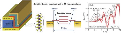
ABSTRACT Two-dimensional (2D) semiconductors are promising candidates for quantum-well devices with the inherent quantum confinement of the subnanometer thickness along the out-of-plane direction. Coulomb/quantum oscillation phenomena have been demonstrated in 2D semiconductors devices, including artificial quantum dots with local electrostatic gating and stacked heterostructure quantum wells. However, the exact quantized energy states, let alone the complexity of the device structures and low observation temperature, have not been clearly revealed. Here, we report a rational fabrication platform of 2D semiconductor nanotransistors to directly construct a Schottky-barrier quantum well (SB-QW) for quantized energy states engineering. The feature size of the quantum well is tailored by a vertical nanochannel of monolayer transition metal dichalcogenides (TMDCs) via an insulating spacer. Meanwhile, the potential barrier is constructed by the Schottky barrier. Quantum oscillations are clearly observed and the quantized energy states are extracted from the source-drain current modulated with the gate bias. Such quantum oscillations are preserved up to ∼100K with a channel length of approximately 16 nm. With an evaluated Schottky barrier height of approximately 27 meV, the quantized energy states are estimated from 2 to 24 meV near the conduction band edge, consistent with corresponding explicit principal quantum numbers. Our work demonstrates the feasibility of moving 2D van der Waals semiconductor nanotransistors towards quantum transistors.
中文翻译:

二维半导体纳米晶体管中的肖特基势垒量子阱
摘要 二维 (2D) 半导体是具有沿面外方向亚纳米厚度的固有量子限制的量子阱器件的有前途的候选者。库仑/量子振荡现象已在二维半导体器件中得到证实,包括具有局部静电门控和堆叠异质结构量子阱的人造量子点。然而,精确的量子化能态,更不用说器件结构的复杂性和低观察温度,还没有被清楚地揭示出来。在这里,我们报告了一个合理的二维半导体纳米晶体管制造平台,以直接构建肖特基势垒量子阱(SB-QW)用于量化能态工程。量子阱的特征尺寸由单层过渡金属二硫属化物 (TMDC) 的垂直纳米通道通过绝缘间隔物定制。同时,势垒由肖特基势垒构成。可以清楚地观察到量子振荡,并且从用栅极偏置调制的源漏电流中提取量子化的能量状态。这种量子振荡在通道长度约为 16 nm 的情况下可保持高达 ~100K。评估的肖特基势垒高度约为 27 meV,估计导带边缘附近的量子化能态为 2 至 24 meV,与相应的显式主量子数一致。我们的工作证明了将 2D 范德华半导体纳米晶体管移向量子晶体管的可行性。同时,势垒由肖特基势垒构成。可以清楚地观察到量子振荡,并且从用栅极偏置调制的源漏电流中提取量子化的能量状态。这种量子振荡在通道长度约为 16 nm 的情况下可保持高达 ~100K。评估的肖特基势垒高度约为 27 meV,估计导带边缘附近的量子化能态为 2 至 24 meV,与相应的显式主量子数一致。我们的工作证明了将 2D 范德华半导体纳米晶体管移向量子晶体管的可行性。同时,势垒由肖特基势垒构成。可以清楚地观察到量子振荡,并且从用栅极偏置调制的源漏电流中提取量子化的能量状态。这种量子振荡在通道长度约为 16 nm 的情况下可保持高达 ~100K。评估的肖特基势垒高度约为 27 meV,估计导带边缘附近的量子化能态为 2 至 24 meV,与相应的显式主量子数一致。我们的工作证明了将 2D 范德华半导体纳米晶体管移向量子晶体管的可行性。可以清楚地观察到量子振荡,并且从用栅极偏置调制的源漏电流中提取量子化的能量状态。这种量子振荡在通道长度约为 16 nm 的情况下可保持高达 ~100K。评估的肖特基势垒高度约为 27 meV,估计导带边缘附近的量子化能态为 2 至 24 meV,与相应的显式主量子数一致。我们的工作证明了将 2D 范德华半导体纳米晶体管移向量子晶体管的可行性。可以清楚地观察到量子振荡,并且从用栅极偏置调制的源漏电流中提取量子化的能量状态。这种量子振荡在通道长度约为 16 nm 的情况下可保持高达 ~100K。评估的肖特基势垒高度约为 27 meV,估计导带边缘附近的量子化能态为 2 至 24 meV,与相应的显式主量子数一致。我们的工作证明了将 2D 范德华半导体纳米晶体管移向量子晶体管的可行性。估计导带边缘附近的量子化能态为 2 到 24 meV,与相应的显式主量子数一致。我们的工作证明了将 2D 范德华半导体纳米晶体管移向量子晶体管的可行性。估计导带边缘附近的量子化能态为 2 到 24 meV,与相应的显式主量子数一致。我们的工作证明了将 2D 范德华半导体纳米晶体管移向量子晶体管的可行性。
更新日期:2020-12-01
中文翻译:
二维半导体纳米晶体管中的肖特基势垒量子阱
摘要 二维 (2D) 半导体是具有沿面外方向亚纳米厚度的固有量子限制的量子阱器件的有前途的候选者。库仑/量子振荡现象已在二维半导体器件中得到证实,包括具有局部静电门控和堆叠异质结构量子阱的人造量子点。然而,精确的量子化能态,更不用说器件结构的复杂性和低观察温度,还没有被清楚地揭示出来。在这里,我们报告了一个合理的二维半导体纳米晶体管制造平台,以直接构建肖特基势垒量子阱(SB-QW)用于量化能态工程。量子阱的特征尺寸由单层过渡金属二硫属化物 (TMDC) 的垂直纳米通道通过绝缘间隔物定制。同时,势垒由肖特基势垒构成。可以清楚地观察到量子振荡,并且从用栅极偏置调制的源漏电流中提取量子化的能量状态。这种量子振荡在通道长度约为 16 nm 的情况下可保持高达 ~100K。评估的肖特基势垒高度约为 27 meV,估计导带边缘附近的量子化能态为 2 至 24 meV,与相应的显式主量子数一致。我们的工作证明了将 2D 范德华半导体纳米晶体管移向量子晶体管的可行性。同时,势垒由肖特基势垒构成。可以清楚地观察到量子振荡,并且从用栅极偏置调制的源漏电流中提取量子化的能量状态。这种量子振荡在通道长度约为 16 nm 的情况下可保持高达 ~100K。评估的肖特基势垒高度约为 27 meV,估计导带边缘附近的量子化能态为 2 至 24 meV,与相应的显式主量子数一致。我们的工作证明了将 2D 范德华半导体纳米晶体管移向量子晶体管的可行性。同时,势垒由肖特基势垒构成。可以清楚地观察到量子振荡,并且从用栅极偏置调制的源漏电流中提取量子化的能量状态。这种量子振荡在通道长度约为 16 nm 的情况下可保持高达 ~100K。评估的肖特基势垒高度约为 27 meV,估计导带边缘附近的量子化能态为 2 至 24 meV,与相应的显式主量子数一致。我们的工作证明了将 2D 范德华半导体纳米晶体管移向量子晶体管的可行性。可以清楚地观察到量子振荡,并且从用栅极偏置调制的源漏电流中提取量子化的能量状态。这种量子振荡在通道长度约为 16 nm 的情况下可保持高达 ~100K。评估的肖特基势垒高度约为 27 meV,估计导带边缘附近的量子化能态为 2 至 24 meV,与相应的显式主量子数一致。我们的工作证明了将 2D 范德华半导体纳米晶体管移向量子晶体管的可行性。可以清楚地观察到量子振荡,并且从用栅极偏置调制的源漏电流中提取量子化的能量状态。这种量子振荡在通道长度约为 16 nm 的情况下可保持高达 ~100K。评估的肖特基势垒高度约为 27 meV,估计导带边缘附近的量子化能态为 2 至 24 meV,与相应的显式主量子数一致。我们的工作证明了将 2D 范德华半导体纳米晶体管移向量子晶体管的可行性。估计导带边缘附近的量子化能态为 2 到 24 meV,与相应的显式主量子数一致。我们的工作证明了将 2D 范德华半导体纳米晶体管移向量子晶体管的可行性。估计导带边缘附近的量子化能态为 2 到 24 meV,与相应的显式主量子数一致。我们的工作证明了将 2D 范德华半导体纳米晶体管移向量子晶体管的可行性。


 京公网安备 11010802027423号