当前位置:
X-MOL 学术
›
Micro Nanostruct.
›
论文详情
Our official English website, www.x-mol.net, welcomes your feedback! (Note: you will need to create a separate account there.)
Thin film NiO/BaTiO3/ZnO heterojunction diode-based UVC photodetectors
Micro and Nanostructures ( IF 3.1 ) Pub Date : 2020-11-01 , DOI: 10.1016/j.spmi.2020.106690 Alaa K. Hassan , Ghusoon M. Ali
Micro and Nanostructures ( IF 3.1 ) Pub Date : 2020-11-01 , DOI: 10.1016/j.spmi.2020.106690 Alaa K. Hassan , Ghusoon M. Ali
|
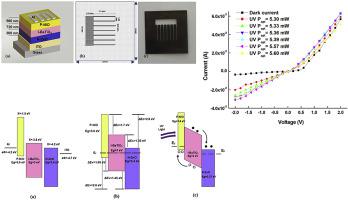
Abstract In this work, a P-I-N thin film Al/NiO/BaTiO3/ZnO/ITO heterojunction diode-based UVC detector was fabricated and characterized. The thin film layers were grown by a low-cost and versatile sol-gel spin coating technique. Scanning electron microscopy (SEM) was utilized to assess the thin film surface microstructure. The crystal structure of the surface layer was investigated by x-ray diffraction (XRD). The P-I-N electrical parameters were estimated from the current-voltage characteristics. The effects of ex situ thermal treatment on the device characteristics were evaluated. The untreated diode showed poor rectifying behavior, and the optimum characteristics were presented by the device treated at 100°C. The P-I-N photodetection capability was studied in the dark and under different optical power radiation levels ranging from 5.3 to 5.6 mW. The photodetection response of the devices treated at the optimum temperature was investigated. Under 5.57 mW UVC (254 nm) illumination and an applied bias of -1.5 V, the P-I-N device demonstrated a photocurrent, contrast ratio, noise equivalent power, and gain of 2.2×10‒2 A, 10, 3.3×10⁻¹⁰ W Hz-1/2, and 19.4, respectively.
中文翻译:

基于薄膜 NiO/BaTiO3/ZnO 异质结二极管的 UVC 光电探测器
摘要 在这项工作中,制备并表征了一种基于 PIN 薄膜 Al/NiO/BaTiO3/ZnO/ITO 异质结二极管的 UVC 探测器。薄膜层是通过低成本和通用的溶胶-凝胶旋涂技术生长的。使用扫描电子显微镜(SEM)来评估薄膜表面微结构。通过X射线衍射(XRD)研究表面层的晶体结构。PIN 电气参数是根据电流-电压特性估算的。评估了非原位热处理对器件特性的影响。未经处理的二极管显示出较差的整流行为,最佳特性由在 100°C 下处理的器件呈现。在黑暗中和在 5.3 至 5.6 mW 的不同光功率辐射水平下研究了 PIN 光电检测能力。研究了在最佳温度下处理的器件的光电检测响应。在 5.57 mW UVC (254 nm) 光照和 -1.5 V 偏置电压下,PIN 器件的光电流、对比度、噪声等效功率和增益分别为 2.2×10⁻² A、10、3.3×10⁻¹⁰ W分别为 Hz-1/2 和 19.4。
更新日期:2020-11-01
中文翻译:
基于薄膜 NiO/BaTiO3/ZnO 异质结二极管的 UVC 光电探测器
摘要 在这项工作中,制备并表征了一种基于 PIN 薄膜 Al/NiO/BaTiO3/ZnO/ITO 异质结二极管的 UVC 探测器。薄膜层是通过低成本和通用的溶胶-凝胶旋涂技术生长的。使用扫描电子显微镜(SEM)来评估薄膜表面微结构。通过X射线衍射(XRD)研究表面层的晶体结构。PIN 电气参数是根据电流-电压特性估算的。评估了非原位热处理对器件特性的影响。未经处理的二极管显示出较差的整流行为,最佳特性由在 100°C 下处理的器件呈现。在黑暗中和在 5.3 至 5.6 mW 的不同光功率辐射水平下研究了 PIN 光电检测能力。研究了在最佳温度下处理的器件的光电检测响应。在 5.57 mW UVC (254 nm) 光照和 -1.5 V 偏置电压下,PIN 器件的光电流、对比度、噪声等效功率和增益分别为 2.2×10⁻² A、10、3.3×10⁻¹⁰ W分别为 Hz-1/2 和 19.4。


 京公网安备 11010802027423号