当前位置:
X-MOL 学术
›
Int. J. Circ. Theory Appl.
›
论文详情
Our official English website, www.x-mol.net, welcomes your feedback! (Note: you will need to create a separate account there.)
A novel flash‐like all‐metal‐oxide semiconductor analog‐to‐digital converter suitable for system on chips systems
International Journal of Circuit Theory and Applications ( IF 2.3 ) Pub Date : 2020-08-28 , DOI: 10.1002/cta.2866 Yasser S. Abdalla 1, 2
International Journal of Circuit Theory and Applications ( IF 2.3 ) Pub Date : 2020-08-28 , DOI: 10.1002/cta.2866 Yasser S. Abdalla 1, 2
Affiliation
|
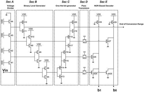
The analog‐to‐digital converters (ADCs) play a very important role in electronic products, radar, communication systems and signal processing, to name such a few. In this paper, a novel all‐metal‐oxide semiconductor (MOS) flash‐like analog‐to‐digital converter (FLADC) that consists of five stages is proposed. The design was performed using only MOS transistors, and the proposed ADC works in a way similar to the conventional flash ADC. According to the proposed ADC, there is no need for the comparators used in the conventional flash ADCs, thus resulting in a reduction in both the transistor count and the power consumption. The sound operation and the superiority of the proposed ADC compared to previous works is verified by simulation using the 0.13‐μm complementary MOS (CMOS) technology with a power‐supply voltage, VDD, of 1.2 V. The simulation has been conducted on a 5‐bit FLADC that is built by 276 MOS transistors only which is approximately 32% of the transistor count of the corresponding conventional flash ADC and has no resistors. According to the simulation results, the proposed 5‐bit FLADC consumes 3.23 mW at sampling rate of 0.5 GS/s.
中文翻译:

一种适用于片上系统的新型闪存状全金属氧化物半导体模数转换器
模数转换器(ADC)在电子产品,雷达,通信系统和信号处理中起着非常重要的作用。本文提出了一种新颖的全金属氧化物半导体(MOS)类闪存模数转换器(FLADC),它由五个阶段组成。该设计仅使用MOS晶体管完成,所提出的ADC的工作方式与传统的Flash ADC相似。根据所提出的ADC,不需要在常规闪存ADC中使用的比较器,从而导致晶体管数量和功耗的减少。通过使用电源电压为V的0.13μm互补MOS(CMOS)技术进行仿真,验证了拟议ADC与以前的作品相比的声音操作和优越性DD为1.2V。仿真是在5位FLADC上进行的,该FLADC仅由276个MOS晶体管构建,大约是相应常规Flash ADC晶体管数量的32%,并且没有电阻。根据仿真结果,建议的5位FLADC在0.5 GS / s的采样率下消耗3.23 mW。
更新日期:2020-11-06
中文翻译:
一种适用于片上系统的新型闪存状全金属氧化物半导体模数转换器
模数转换器(ADC)在电子产品,雷达,通信系统和信号处理中起着非常重要的作用。本文提出了一种新颖的全金属氧化物半导体(MOS)类闪存模数转换器(FLADC),它由五个阶段组成。该设计仅使用MOS晶体管完成,所提出的ADC的工作方式与传统的Flash ADC相似。根据所提出的ADC,不需要在常规闪存ADC中使用的比较器,从而导致晶体管数量和功耗的减少。通过使用电源电压为V的0.13μm互补MOS(CMOS)技术进行仿真,验证了拟议ADC与以前的作品相比的声音操作和优越性DD为1.2V。仿真是在5位FLADC上进行的,该FLADC仅由276个MOS晶体管构建,大约是相应常规Flash ADC晶体管数量的32%,并且没有电阻。根据仿真结果,建议的5位FLADC在0.5 GS / s的采样率下消耗3.23 mW。


 京公网安备 11010802027423号