当前位置:
X-MOL 学术
›
ACS Appl. Electron. Mater.
›
论文详情
Our official English website, www.x-mol.net, welcomes your feedback! (Note: you will need to create a separate account there.)
Epitaxial High-Yield Intrinsic and Te-Doped Dilute Nitride GaAsSbN Nanowire Heterostructure and Ensemble Photodetector Application
ACS Applied Electronic Materials ( IF 4.7 ) Pub Date : 2020-08-27 , DOI: 10.1021/acsaelm.0c00450 Rabin Pokharel 1 , Priyanka Ramaswamy 2 , Shisir Devkota 1 , Mehul Parakh 1 , Kendall Dawkins 1 , Aubrey Penn 3, 4 , Matthew Cabral 3, 4 , Lewis Reynolds 3 , Shanthi Iyer 1
ACS Applied Electronic Materials ( IF 4.7 ) Pub Date : 2020-08-27 , DOI: 10.1021/acsaelm.0c00450 Rabin Pokharel 1 , Priyanka Ramaswamy 2 , Shisir Devkota 1 , Mehul Parakh 1 , Kendall Dawkins 1 , Aubrey Penn 3, 4 , Matthew Cabral 3, 4 , Lewis Reynolds 3 , Shanthi Iyer 1
Affiliation
|
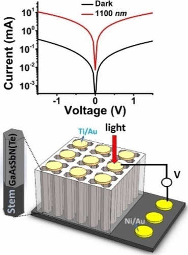
Band gap engineering of GaAsSbN nanowires (NWs) grown by Ga-assisted molecular beam epitaxy and demonstration of a Te-doped axial GaAsSbN NW-based Schottky barrier photodetector on p-Si (111) in the near-infrared region are reported. Stringent control on NW nucleation conditions, stem growth duration, and NW exposure to the N-plasma were found to be critical for the successful growth of high-quality dilute nitride quaternary GaAsSbN NWs in the axial configuration. Planar defect-free structures were realized with room temperature photoluminescence (PL) characteristics, revealing reduced N-induced point defects and nonradiative recombination centers. N incorporation in the dilute nitride NWs was ascertained from PL and Raman spectral mode shifts and shapes and weak temperature-dependent PL peak energy. The advantage of Te-doping in dilute nitride NWs using a GaTe captive source is the compensation of point defects, as evidenced by a significant improvement in PL characteristics, Raman mode shifts, and spectral shape, with improved photodetector device performance relative to intrinsic dilute nitride NWs. Te-doped GaAsSbN NW Schottky-based photodetectors have been demonstrated on both single and ensemble configurations with a resultant responsivity of 5 A/W at 860 nm and 3800 A/W at 1100, respectively. Detectivity of 3.2 × 10¹⁰ Jones was achieved on the Te-doped ensemble NW device. The findings presented in this work showcase prospects for rich band gap engineering using doped GaAsSbN NWs for near-infrared region device applications.
中文翻译:

外延高产本征和掺Te稀氮化物GaAsSbN纳米线异质结构及集成光电探测器的应用
报道了通过Ga辅助分子束外延生长的GaAsSbN纳米线(NW)的带隙工程,并在近红外区域的p-Si(111)上演示了Te掺杂的轴向GaAsSbN NW基肖特基势垒光电探测器。已发现严格控制NW成核条件,茎生长持续时间以及NW暴露于N-等离子体对于高质量,高纯度的氮化物季铵GaAsSbN NW在轴向构型中的成功生长至关重要。实现了具有室温光致发光(PL)特性的平面无缺陷结构,揭示了减少的N诱导点缺陷和非辐射复合中心。从PL和拉曼光谱模式移动和形状以及与温度相关的PL峰值能量弱确定了稀氮化物NW中的N掺入。使用GaTe俘获源在稀氮化物NW中掺杂Te的优点是可以补偿点缺陷,这可以通过PL特性,拉曼模式位移和光谱形状的显着改善来证明,相对于本征稀氮化物,光电探测器的性能得到了改善西北。Te掺杂的GaAsSbN NW肖特基光电探测器已经在单一和整体配置上得到了证明,其结果分别在860 nm和1100 nm的响应率为5 A / W和3800 A / W。探测灵敏度为3.2×10 Te掺杂的GaAsSbN NW肖特基光电探测器已经在单一和整体配置上得到了证明,其结果分别在860 nm和1100 nm的响应率为5 A / W和3800 A / W。探测灵敏度为3.2×10 Te掺杂的GaAsSbN NW肖特基光电探测器已经在单一和整体配置上得到了证明,其结果分别在860 nm和1100 nm的响应率为5 A / W和3800 A / W。探测灵敏度为3.2×10在Te掺杂的整体NW器件上达到了10 Jones。这项工作中提出的发现展示了使用掺杂的GaAsSbN NW进行近红外区域器件应用的富带隙工程的前景。
更新日期:2020-09-22
中文翻译:
外延高产本征和掺Te稀氮化物GaAsSbN纳米线异质结构及集成光电探测器的应用
报道了通过Ga辅助分子束外延生长的GaAsSbN纳米线(NW)的带隙工程,并在近红外区域的p-Si(111)上演示了Te掺杂的轴向GaAsSbN NW基肖特基势垒光电探测器。已发现严格控制NW成核条件,茎生长持续时间以及NW暴露于N-等离子体对于高质量,高纯度的氮化物季铵GaAsSbN NW在轴向构型中的成功生长至关重要。实现了具有室温光致发光(PL)特性的平面无缺陷结构,揭示了减少的N诱导点缺陷和非辐射复合中心。从PL和拉曼光谱模式移动和形状以及与温度相关的PL峰值能量弱确定了稀氮化物NW中的N掺入。使用GaTe俘获源在稀氮化物NW中掺杂Te的优点是可以补偿点缺陷,这可以通过PL特性,拉曼模式位移和光谱形状的显着改善来证明,相对于本征稀氮化物,光电探测器的性能得到了改善西北。Te掺杂的GaAsSbN NW肖特基光电探测器已经在单一和整体配置上得到了证明,其结果分别在860 nm和1100 nm的响应率为5 A / W和3800 A / W。探测灵敏度为3.2×10 Te掺杂的GaAsSbN NW肖特基光电探测器已经在单一和整体配置上得到了证明,其结果分别在860 nm和1100 nm的响应率为5 A / W和3800 A / W。探测灵敏度为3.2×10 Te掺杂的GaAsSbN NW肖特基光电探测器已经在单一和整体配置上得到了证明,其结果分别在860 nm和1100 nm的响应率为5 A / W和3800 A / W。探测灵敏度为3.2×10在Te掺杂的整体NW器件上达到了10 Jones。这项工作中提出的发现展示了使用掺杂的GaAsSbN NW进行近红外区域器件应用的富带隙工程的前景。


 京公网安备 11010802027423号