当前位置:
X-MOL 学术
›
Adv. Electron. Mater.
›
论文详情
Our official English website, www.x-mol.net, welcomes your feedback! (Note: you will need to create a separate account there.)
Controllable p‐to‐n Type Conductance Transition in Top‐Gated Graphene Field Effect Transistor by Interface Trap Engineering
Advanced Electronic Materials ( IF 6.2 ) Pub Date : 2020-08-19 , DOI: 10.1002/aelm.202000496 Songang Peng 1, 2 , Zhi Jin 1 , Yao Yao 1 , Xinnan Huang 1 , Dayong Zhang 1, 2 , Jiebin Niu 2 , Jingyuan Shi 1 , Yanhui Zhang 3 , Guanghui Yu 3
Advanced Electronic Materials ( IF 6.2 ) Pub Date : 2020-08-19 , DOI: 10.1002/aelm.202000496 Songang Peng 1, 2 , Zhi Jin 1 , Yao Yao 1 , Xinnan Huang 1 , Dayong Zhang 1, 2 , Jiebin Niu 2 , Jingyuan Shi 1 , Yanhui Zhang 3 , Guanghui Yu 3
Affiliation
|
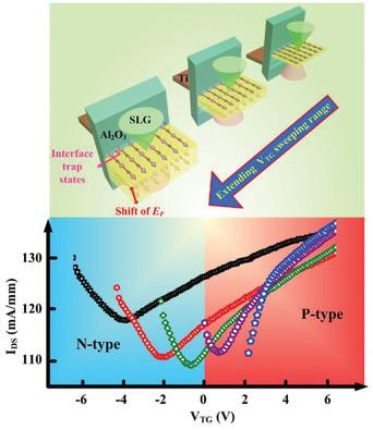
Modulating the electronic property of graphene by doping is essential for its device and circuit applications. Unfortunately, controllable p‐ and n‐type doping in top‐gated graphene field effect transistor (GFET) is reported. Here, the O3‐based atomic layer deposited Al2O3 layer as top gate dielectric is chosen. The epoxide functional group formed in the O3 process serves as effective interface trap sites. As the sweeping range of top gate voltage increases, the Dirac point position of GFET moves from positive voltage to negative voltage. The shift of the Dirac point voltage indicates the doping transition of graphene from p‐type to n‐type. The gate voltage dependent doping can be attributed to the charge exchange between graphene and interface trap sites. Furthermore, a trap‐dependent charge model is proposed to explain the transport mechanism in the doping process. This approach is promising to produce the complementary p‐ and n‐type top‐gated GFET for multiple applications.
中文翻译:

通过界面陷阱工程技术可控制顶部石墨烯场效应晶体管中的p至n型电导转换
通过掺杂调节石墨烯的电子性能对其设备和电路应用至关重要。不幸的是,据报道在顶部栅极的石墨烯场效应晶体管(GFET)中可控的p型和n型掺杂。在这里,选择基于O 3的原子层沉积的Al 2 O 3层作为顶栅电介质。在O 3中形成的环氧官能团过程充当有效的界面陷阱站点。随着顶部栅极电压扫描范围的增加,GFET的狄拉克点位置将从正电压移至负电压。狄拉克点电压的变化表明石墨烯从p型到n型的掺杂跃迁。栅极电压相关的掺杂可归因于石墨烯和界面陷阱位点之间的电荷交换。此外,提出了一种依赖陷阱的电荷模型来解释掺杂过程中的传输机制。这种方法有望为多种应用生产互补的p型和n型顶部栅极GFET。
更新日期:2020-09-08
中文翻译:
通过界面陷阱工程技术可控制顶部石墨烯场效应晶体管中的p至n型电导转换
通过掺杂调节石墨烯的电子性能对其设备和电路应用至关重要。不幸的是,据报道在顶部栅极的石墨烯场效应晶体管(GFET)中可控的p型和n型掺杂。在这里,选择基于O 3的原子层沉积的Al 2 O 3层作为顶栅电介质。在O 3中形成的环氧官能团过程充当有效的界面陷阱站点。随着顶部栅极电压扫描范围的增加,GFET的狄拉克点位置将从正电压移至负电压。狄拉克点电压的变化表明石墨烯从p型到n型的掺杂跃迁。栅极电压相关的掺杂可归因于石墨烯和界面陷阱位点之间的电荷交换。此外,提出了一种依赖陷阱的电荷模型来解释掺杂过程中的传输机制。这种方法有望为多种应用生产互补的p型和n型顶部栅极GFET。


 京公网安备 11010802027423号