当前位置:
X-MOL 学术
›
J. Chin. Chem. Soc.
›
论文详情
Our official English website, www.x-mol.net, welcomes your feedback! (Note: you will need to create a separate account there.)
Semiconductor nanocrystals possessing broadly size‐ and facet‐dependent optical properties
Journal of the Chinese Chemical Society ( IF 1.8 ) Pub Date : 2020-08-17 , DOI: 10.1002/jccs.202000267 Michael H. Huang
Journal of the Chinese Chemical Society ( IF 1.8 ) Pub Date : 2020-08-17 , DOI: 10.1002/jccs.202000267 Michael H. Huang
|
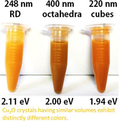
Cu2O cubes, octahedra, and rhombic dodecahedra have been shown to exhibit continuous light absorption and emission band shifts with increasing particle sizes from 10 nm to sub‐microcrystals. They also possess clear facet‐dependent optical properties. Ag3PO4, Ag2O, SrTiO3, and CeO2 crystals show similar optical size and facet effects. Thus, spectral shifts over a broad size range far beyond the quantum‐size regime should be generally observable in many semiconductor materials. Facet‐dependent optical properties of a semiconductor can be understood to arise from the presence of an ultrathin surface layer with subtle bond and orbital level variations for different crystal faces. Although these optical features seem unexpected, they should be the general behaviors of semiconductor crystals. As more examples of these optical effects are available, we will find that these intrinsic properties of semiconductors have been ignored in the past. Furthermore, if valence and conduction band positions are broadly tunable by particle size, the knowledge should have tremendous impacts on the applications of semiconductors, where band energies are important to efficient interfacial charge transfer.
中文翻译:

半导体纳米晶体具有广泛的尺寸和刻面相关光学特性
已经证明,Cu 2 O立方体,八面体和菱形十二面体在从10 nm到亚微晶的粒径增加时,表现出连续的光吸收和发射带移。它们还具有清晰的面相关光学特性。Ag 3 PO 4,Ag 2 O,SrTiO 3和CeO 2晶体显示出相似的光学尺寸和刻面效果。因此,在许多半导体材料中通常应观察到远远超出量子尺寸范围的宽范围光谱变化。半导体的取决于面的光学特性可以理解为是由于存在超薄表面层而导致的,该表面层具有微妙的键合和不同晶体面的轨道能级变化。尽管这些光学特征似乎是出乎意料的,但它们应该是半导体晶体的一般行为。随着这些光学效应的更多实例的出现,我们将发现过去半导体的这些固有特性已被忽略。此外,如果价和导带位置可以通过粒径大体上进行调节,那么这些知识将对半导体的应用产生巨大影响,
更新日期:2020-08-17
中文翻译:
半导体纳米晶体具有广泛的尺寸和刻面相关光学特性
已经证明,Cu 2 O立方体,八面体和菱形十二面体在从10 nm到亚微晶的粒径增加时,表现出连续的光吸收和发射带移。它们还具有清晰的面相关光学特性。Ag 3 PO 4,Ag 2 O,SrTiO 3和CeO 2晶体显示出相似的光学尺寸和刻面效果。因此,在许多半导体材料中通常应观察到远远超出量子尺寸范围的宽范围光谱变化。半导体的取决于面的光学特性可以理解为是由于存在超薄表面层而导致的,该表面层具有微妙的键合和不同晶体面的轨道能级变化。尽管这些光学特征似乎是出乎意料的,但它们应该是半导体晶体的一般行为。随着这些光学效应的更多实例的出现,我们将发现过去半导体的这些固有特性已被忽略。此外,如果价和导带位置可以通过粒径大体上进行调节,那么这些知识将对半导体的应用产生巨大影响,


 京公网安备 11010802027423号