当前位置:
X-MOL 学术
›
Adv. Electron. Mater.
›
论文详情
Our official English website, www.x-mol.net, welcomes your feedback! (Note: you will need to create a separate account there.)
Wafer‐Scale Organic Complementary Inverters Fabricated with Self‐Assembled Monolayer Field‐Effect Transistors
Advanced Electronic Materials ( IF 6.2 ) Pub Date : 2020-08-06 , DOI: 10.1002/aelm.202000515 Baolin Zhao 1 , Bastian Gothe 1 , Marco Sarcletti 1 , Yuhan Zhao 1 , Tobias Rejek 1 , Xin Liu 2 , Hyoungwon Park 1 , Peter Strohriegl 3 , Marcus Halik 1
Advanced Electronic Materials ( IF 6.2 ) Pub Date : 2020-08-06 , DOI: 10.1002/aelm.202000515 Baolin Zhao 1 , Bastian Gothe 1 , Marco Sarcletti 1 , Yuhan Zhao 1 , Tobias Rejek 1 , Xin Liu 2 , Hyoungwon Park 1 , Peter Strohriegl 3 , Marcus Halik 1
Affiliation
|
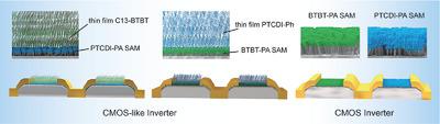
Self‐assembled monolayers (SAMs) of π‐conjugated molecules can achieve robust charge transport by the formation of ordered 2D layers at the desired regions, which enable their application for organic integrated circuits. Here, the self‐assembled monolayer field‐effect transistor concept is applied as a scalable method to realize fully integrated complementary inverters by stepwise semiconductor deposition. Two‐component stacked bilayer ambipolar transistors are fabricated by semiconducting self‐assembled monolayers (n‐SAM or p‐SAM) as the bottom layer and a complementary thin‐film semiconductor layer on top. The integrated complementary metal‐oxide‐semiconductor like (CMOS‐like) inverter achieves proper logic performances. The nanometer‐thin monolayers exhibit effective charge transport and their flat, homogeneous surfaces benefit the interconnected growth of the top layer. Furthermore, by controlling the solution‐based and region‐selective deposition of p‐ and n‐type SAMs, fully integrated CMOS inverters are realized on wafer scale by photolithography for the first time. The CMOS inverters show a nearly 100% yield with a gain up to 48, and noise margin 3.68 V (73.6% of VDD/2). The strategy of semiconducting SAMs for digital logic gates demonstrates a reliable approach for sophisticated large‐area circuits.
中文翻译:

自组装单层场效应晶体管制成的晶圆级有机互补逆变器
π共轭分子的自组装单分子层(SAMs)可以通过在所需区域形成有序的2D层来实现强大的电荷传输,从而使其能够用于有机集成电路。在这里,自组装单层场效应晶体管的概念被用作可扩展的方法,以通过逐步的半导体沉积来实现完全集成的互补反相器。两组分堆叠式双层双极晶体管是通过将半导体自组装单层(n-SAM或p-SAM)作为底层,并在其顶部形成互补的薄膜半导体层而制成的。集成的类互补金属氧化物半导体(CMOS)反相器可实现适当的逻辑性能。纳米薄的单分子层具有有效的电荷传输能力,其平坦,均匀的表面有利于顶层的互连生长。此外,通过控制p型和n型SAM的基于溶液的选择沉积和区域选择沉积,首次通过光刻技术在晶圆级实现了完全集成的CMOS反相器。CMOS反相器显示出近100%的良率,增益高达48,噪声容限为3.68 V(V的73.6%DD / 2)。用于数字逻辑门的半导体SAM策略展示了一种用于复杂的大面积电路的可靠方法。
更新日期:2020-09-08
中文翻译:
自组装单层场效应晶体管制成的晶圆级有机互补逆变器
π共轭分子的自组装单分子层(SAMs)可以通过在所需区域形成有序的2D层来实现强大的电荷传输,从而使其能够用于有机集成电路。在这里,自组装单层场效应晶体管的概念被用作可扩展的方法,以通过逐步的半导体沉积来实现完全集成的互补反相器。两组分堆叠式双层双极晶体管是通过将半导体自组装单层(n-SAM或p-SAM)作为底层,并在其顶部形成互补的薄膜半导体层而制成的。集成的类互补金属氧化物半导体(CMOS)反相器可实现适当的逻辑性能。纳米薄的单分子层具有有效的电荷传输能力,其平坦,均匀的表面有利于顶层的互连生长。此外,通过控制p型和n型SAM的基于溶液的选择沉积和区域选择沉积,首次通过光刻技术在晶圆级实现了完全集成的CMOS反相器。CMOS反相器显示出近100%的良率,增益高达48,噪声容限为3.68 V(V的73.6%DD / 2)。用于数字逻辑门的半导体SAM策略展示了一种用于复杂的大面积电路的可靠方法。


 京公网安备 11010802027423号