当前位置:
X-MOL 学术
›
Prog. Photovoltaics
›
论文详情
Our official English website, www.x-mol.net, welcomes your feedback! (Note: you will need to create a separate account there.)
Theoretical and experimental assessment of thinned germanium substrates for III–V multijunction solar cells
Progress in Photovoltaics ( IF 6.7 ) Pub Date : 2020-07-29 , DOI: 10.1002/pip.3281 Iván Lombardero 1 , Mario Ochoa 1 , Naoya Miyashita 2 , Yoshitaka Okada 2 , Carlos Algora 1
Progress in Photovoltaics ( IF 6.7 ) Pub Date : 2020-07-29 , DOI: 10.1002/pip.3281 Iván Lombardero 1 , Mario Ochoa 1 , Naoya Miyashita 2 , Yoshitaka Okada 2 , Carlos Algora 1
Affiliation
|
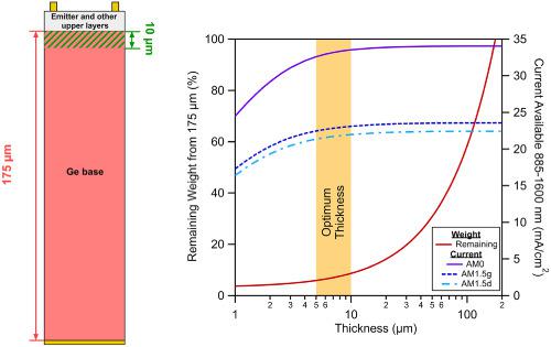
Solar cells manufactured on top of Ge substrates suffer from inherent drawbacks that hinder or limit their potential. The most deleterious ones are heavy weight, high bulk recombination, lack of photon confinement, and an increase of the heat absorption. The use of thinned Ge substrates is herein proposed as a possible solution to the aforementioned challenges. The potential of a thinned Ge subcell inside a standard GaInP/Ga(In)As/Ge triple‐junction solar cell is assessed by simulations, pointing to an optimum thickness around 5–10 μm. This would reduce the weight by more than 90%, whereas the available current for the Ge subcell would decrease only by 5%. In addition, the heat absorption for wavelengths beyond 1600 nm would decrease by more than 85%. The performance of such a device is highly influenced by the front and back surface recombination of the p–n junction. Simulations remark that good back surface passivation is mandatory to avoid losing power generation by thinning the substrate. In contrast, it has been found that front surface recombination lowers the power generation in a similar manner for thin and thick solar cells. Therefore, the benefits of thinning the substrate are not limited by the front surface recombination. Finally, Ge single‐junction solar cells thinned down to 85 μm by wet etching processes are demonstrated. The feasibility of the thinning process is supported by the limited losses measured in the current generation (less than 6%) and generated voltage (4%) for the thinnest solar cell manufactured.
中文翻译:

用于III–V多结太阳能电池的薄锗衬底的理论和实验评估
在Ge衬底顶部制造的太阳能电池具有固有的缺陷,这些缺陷会阻碍或限制其潜力。最有害的是重量重,大量重组,缺乏光子限制以及吸热增加。本文提出了使用减薄的Ge衬底作为上述挑战的可能解决方案。通过仿真评估了标准GaInP / Ga(In)As / Ge三结太阳能电池内部的Ge子电池变薄的潜力,并指出了5-10μm左右的最佳厚度。这将使重量减少90%以上,而Ge子电池的可用电流仅减少5%。此外,超过1600 nm的波长的热吸收将减少超过85%。这种器件的性能在很大程度上受到p–n结的前表面和后表面复合的影响。仿真表明,良好的背面钝化是必不可少的,以避免通过减薄衬底而损失功率。相反,已经发现,前表面复合以类似的方式降低了薄型和厚型太阳能电池的发电量。因此,使基板变薄的益处不受前表面复合的限制。最后,展示了通过湿法刻蚀工艺将其薄化至85μm的Ge单结太阳能电池。对于制造的最薄的太阳能电池,电流测量(小于6%)和发电电压(4%)的有限损失支持了减薄工艺的可行性。仿真表明,良好的背面钝化是必不可少的,以避免通过减薄衬底而损失功率。相反,已经发现,对于薄和厚的太阳能电池,前表面复合以类似的方式降低了发电量。因此,使基板变薄的益处不受前表面复合的限制。最后,展示了通过湿法刻蚀工艺将其薄化至85μm的Ge单结太阳能电池。对于制造的最薄的太阳能电池,电流测量(小于6%)和发电电压(4%)的有限损失支持了减薄工艺的可行性。仿真表明,良好的背面钝化是必不可少的,以避免通过减薄衬底而损失功率。相反,已经发现,对于薄和厚的太阳能电池,前表面复合以类似的方式降低了发电量。因此,使基板变薄的益处不受前表面复合的限制。最后,展示了通过湿法刻蚀工艺将其薄化至85μm的Ge单结太阳能电池。对于制造的最薄的太阳能电池,电流测量(小于6%)和发电电压(4%)的有限损失支持了减薄工艺的可行性。已经发现,对于薄和厚的太阳能电池,前表面重组以类似的方式降低了发电量。因此,使基板变薄的益处不受前表面复合的限制。最后,展示了通过湿法刻蚀工艺将其薄化至85μm的Ge单结太阳能电池。对于制造的最薄的太阳能电池,电流测量(小于6%)和发电电压(4%)所测得的有限损耗支持了减薄工艺的可行性。已经发现,对于薄和厚的太阳能电池,前表面重组以类似的方式降低了发电量。因此,使基板变薄的益处不受前表面复合的限制。最后,展示了通过湿法刻蚀工艺将其薄化至85μm的Ge单结太阳能电池。对于制造的最薄的太阳能电池,电流测量(小于6%)和发电电压(4%)的有限损失支持了减薄工艺的可行性。
更新日期:2020-10-05
中文翻译:
用于III–V多结太阳能电池的薄锗衬底的理论和实验评估
在Ge衬底顶部制造的太阳能电池具有固有的缺陷,这些缺陷会阻碍或限制其潜力。最有害的是重量重,大量重组,缺乏光子限制以及吸热增加。本文提出了使用减薄的Ge衬底作为上述挑战的可能解决方案。通过仿真评估了标准GaInP / Ga(In)As / Ge三结太阳能电池内部的Ge子电池变薄的潜力,并指出了5-10μm左右的最佳厚度。这将使重量减少90%以上,而Ge子电池的可用电流仅减少5%。此外,超过1600 nm的波长的热吸收将减少超过85%。这种器件的性能在很大程度上受到p–n结的前表面和后表面复合的影响。仿真表明,良好的背面钝化是必不可少的,以避免通过减薄衬底而损失功率。相反,已经发现,前表面复合以类似的方式降低了薄型和厚型太阳能电池的发电量。因此,使基板变薄的益处不受前表面复合的限制。最后,展示了通过湿法刻蚀工艺将其薄化至85μm的Ge单结太阳能电池。对于制造的最薄的太阳能电池,电流测量(小于6%)和发电电压(4%)的有限损失支持了减薄工艺的可行性。仿真表明,良好的背面钝化是必不可少的,以避免通过减薄衬底而损失功率。相反,已经发现,对于薄和厚的太阳能电池,前表面复合以类似的方式降低了发电量。因此,使基板变薄的益处不受前表面复合的限制。最后,展示了通过湿法刻蚀工艺将其薄化至85μm的Ge单结太阳能电池。对于制造的最薄的太阳能电池,电流测量(小于6%)和发电电压(4%)的有限损失支持了减薄工艺的可行性。仿真表明,良好的背面钝化是必不可少的,以避免通过减薄衬底而损失功率。相反,已经发现,对于薄和厚的太阳能电池,前表面复合以类似的方式降低了发电量。因此,使基板变薄的益处不受前表面复合的限制。最后,展示了通过湿法刻蚀工艺将其薄化至85μm的Ge单结太阳能电池。对于制造的最薄的太阳能电池,电流测量(小于6%)和发电电压(4%)的有限损失支持了减薄工艺的可行性。已经发现,对于薄和厚的太阳能电池,前表面重组以类似的方式降低了发电量。因此,使基板变薄的益处不受前表面复合的限制。最后,展示了通过湿法刻蚀工艺将其薄化至85μm的Ge单结太阳能电池。对于制造的最薄的太阳能电池,电流测量(小于6%)和发电电压(4%)所测得的有限损耗支持了减薄工艺的可行性。已经发现,对于薄和厚的太阳能电池,前表面重组以类似的方式降低了发电量。因此,使基板变薄的益处不受前表面复合的限制。最后,展示了通过湿法刻蚀工艺将其薄化至85μm的Ge单结太阳能电池。对于制造的最薄的太阳能电池,电流测量(小于6%)和发电电压(4%)的有限损失支持了减薄工艺的可行性。


 京公网安备 11010802027423号