当前位置:
X-MOL 学术
›
Phys. Status Solidi A
›
论文详情
Our official English website, www.x-mol.net, welcomes your feedback! (Note: you will need to create a separate account there.)
Growth and Properties of N‐Polar InN/InAlN Heterostructures
Physica Status Solidi (A) - Applications and Materials Science ( IF 2 ) Pub Date : 2020-07-28 , DOI: 10.1002/pssa.202000197 Stanislav Hasenöhrl 1 , Edmund Dobročka 1 , Roman Stoklas 1 , Filip Gucmann 1 , Alica Rosová 1 , Jan Kuzmík 1
Physica Status Solidi (A) - Applications and Materials Science ( IF 2 ) Pub Date : 2020-07-28 , DOI: 10.1002/pssa.202000197 Stanislav Hasenöhrl 1 , Edmund Dobročka 1 , Roman Stoklas 1 , Filip Gucmann 1 , Alica Rosová 1 , Jan Kuzmík 1
Affiliation
|
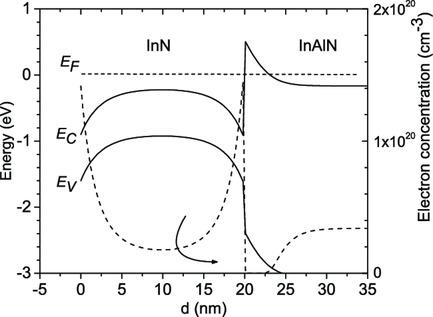
N‐polar InN/InAlN heterostructure growth and performance are studied on‐ and off‐axis sapphire substrates misoriented toward the m or a plane by 4°. A high In molar fraction (0.57) in the InAlN layer is chosen to reduce the lattice mismatch. InN growth on the on‐axis InAlN/sapphire system is initiated with random island formation, which coalesce at ≈10 nm thickness smearing grain boundaries. In contrast, on off‐axis sapphires, growth is defined by misorientation‐induced steps and grains remain visible even after the layer coalesces. The best electron mobility of 720 cm2 V−1 s−1 and carrier density of ≈1.5 × 1019 cm−3 are demonstrated on the heterostructure grown on‐axis sapphire, with InN as thin as 20 nm, even though the InN/InAlN interface root mean square roughness is ≈1.3 nm. The concentrations of screw and edge dislocations in the 20 nm thick InN grown on the on‐axis system are extracted to be 4.7 × 10⁹ and 3.5 × 1010 cm−2. In all cases, the InN lattice is still partially strained, performing only ≈85% relaxation. Further lowering of the lattice mismatch, smoothing of the InAlN surface, and achieving semi‐insulating InAlN will provide necessary development steps toward predicted InN‐channel transistors with unprecedented performance.
中文翻译:

N极性InN / InAlN异质结构的生长和性质
N极性的InN /异质结构的InAlN生长和性能进行了研究轴上和偏轴蓝宝石衬底朝向取向错误的米或一个由4平面°。选择InAlN层中的高In摩尔分数(0.57)以减少晶格失配。轴上InAlN /蓝宝石系统上的InN生长以无序的岛形成开始,该岛在约10 nm的厚度处聚结并涂抹了晶界。相比之下,在偏轴蓝宝石上,生长是由取向失调引起的阶跃确定的,即使层合并后,晶粒仍然可见。最佳电子迁移率为720 cm 2 V -1 s -1,载流子密度为≈1.5×10 19 cm -3在InS薄至20 nm的蓝宝石上生长的异质结构上得到了证明,即使InN / InAlN界面的均方根粗糙度约为1.3 nm。在同轴系统上生长的20 nm厚InN中,螺钉和边缘位错的浓度被提取为4.7×10 9和3.5×10 10 cm -2。在所有情况下,InN晶格仍然部分应变,仅执行≈85%的弛豫。进一步降低晶格失配,InAlN表面光滑和实现半绝缘InAlN,将为预测具有前所未有性能的InN沟道晶体管提供必要的开发步骤。
更新日期:2020-07-28
中文翻译:
N极性InN / InAlN异质结构的生长和性质
N极性的InN /异质结构的InAlN生长和性能进行了研究轴上和偏轴蓝宝石衬底朝向取向错误的米或一个由4平面°。选择InAlN层中的高In摩尔分数(0.57)以减少晶格失配。轴上InAlN /蓝宝石系统上的InN生长以无序的岛形成开始,该岛在约10 nm的厚度处聚结并涂抹了晶界。相比之下,在偏轴蓝宝石上,生长是由取向失调引起的阶跃确定的,即使层合并后,晶粒仍然可见。最佳电子迁移率为720 cm 2 V -1 s -1,载流子密度为≈1.5×10 19 cm -3在InS薄至20 nm的蓝宝石上生长的异质结构上得到了证明,即使InN / InAlN界面的均方根粗糙度约为1.3 nm。在同轴系统上生长的20 nm厚InN中,螺钉和边缘位错的浓度被提取为4.7×10 9和3.5×10 10 cm -2。在所有情况下,InN晶格仍然部分应变,仅执行≈85%的弛豫。进一步降低晶格失配,InAlN表面光滑和实现半绝缘InAlN,将为预测具有前所未有性能的InN沟道晶体管提供必要的开发步骤。


 京公网安备 11010802027423号