当前位置:
X-MOL 学术
›
Phys. Status Solidi A
›
论文详情
Our official English website, www.x-mol.net, welcomes your feedback! (Note: you will need to create a separate account there.)
Metal–Semiconductor–Metal Thin‐Film X‐Ray Detector Based on Halide Perovskites
Physica Status Solidi (A) - Applications and Materials Science ( IF 2 ) Pub Date : 2020-07-25 , DOI: 10.1002/pssa.202000296 Zhaohui Yang 1 , Kaige Wen 1 , Hai Lin 1
Physica Status Solidi (A) - Applications and Materials Science ( IF 2 ) Pub Date : 2020-07-25 , DOI: 10.1002/pssa.202000296 Zhaohui Yang 1 , Kaige Wen 1 , Hai Lin 1
Affiliation
|
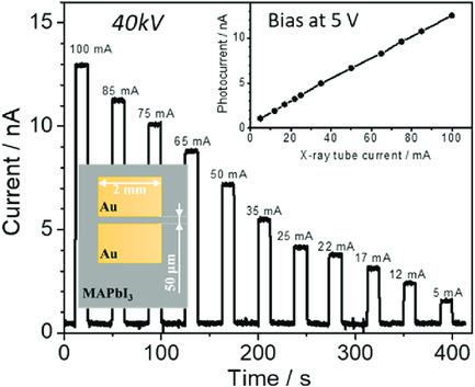
Halide perovskite materials as emerging optoelectronic materials are very appealing for the X‐ray detection due to their superior charge transport, high‐absorption cross section for X‐rays and solution processability. Herein, thin‐film X‐ray detectors are demonstrated using methylammonium lead iodide perovskite (MAPbI3) thin films. Controlled nucleation of halide perovskites is realized using patterned Au dots as nucleation promoters, resulting in uniform thin films with large grains. A metal–semiconductor–metal (MSM) device architecture with coplanar electrodes is used, and the thin‐film detectors with an active layer thickness of 700 nm exhibit a sensitivity of 2.48 × 10⁻² μC Gyair−1 cm−2 under a bias of 10 V. The device is relatively stable in air without encapsulation, showing no degradation after 15 min continuous biasing at 5 V. Such solution‐based perovskite detector can enable X‐ray detecting and imaging with low‐cost, high efficiency, and high sensitivity.
中文翻译:

基于卤化物钙钛矿的金属-半导体-金属薄膜X射线检测器
卤化钙钛矿材料作为新兴的光电材料,由于其优异的电荷传输,X射线的高吸收截面以及溶液的可加工性,在X射线检测中非常有吸引力。本文中,使用甲基铵碘化铅钙钛矿(MAPbI 3)薄膜演示了薄膜X射线检测器。卤化钙钛矿的受控成核是通过使用图案化的Au点作为成核促进剂来实现的,从而得到具有大晶粒的均匀薄膜。金属-半导体-金属(MSM)具有共平面的电极设备体系结构被使用,并且具有700的有源层厚度薄膜探测器纳米表现出2.48×10灵敏度-2 μC戈瑞空气-1 厘米-2 在10 V的偏压下,该器件在空气中相对稳定,无需封装,在5 V的连续偏压下15分钟后,不会显示退化。这种基于溶液的钙钛矿检测器可以低成本,高效率地进行X射线检测和成像,并且灵敏度高。
更新日期:2020-07-25
中文翻译:
基于卤化物钙钛矿的金属-半导体-金属薄膜X射线检测器
卤化钙钛矿材料作为新兴的光电材料,由于其优异的电荷传输,X射线的高吸收截面以及溶液的可加工性,在X射线检测中非常有吸引力。本文中,使用甲基铵碘化铅钙钛矿(MAPbI 3)薄膜演示了薄膜X射线检测器。卤化钙钛矿的受控成核是通过使用图案化的Au点作为成核促进剂来实现的,从而得到具有大晶粒的均匀薄膜。金属-半导体-金属(MSM)具有共平面的电极设备体系结构被使用,并且具有700的有源层厚度薄膜探测器纳米表现出2.48×10灵敏度-2 μC戈瑞空气-1 厘米-2 在10 V的偏压下,该器件在空气中相对稳定,无需封装,在5 V的连续偏压下15分钟后,不会显示退化。这种基于溶液的钙钛矿检测器可以低成本,高效率地进行X射线检测和成像,并且灵敏度高。


 京公网安备 11010802027423号